Philips Semiconductors | TDA8943SF |
| 7 W mono BTL audio amplifier |
Operating — | In this mode the amplifier is operating normally. The operating mode is |
activated at VMODE < 0.5 V.
9. Limiting values
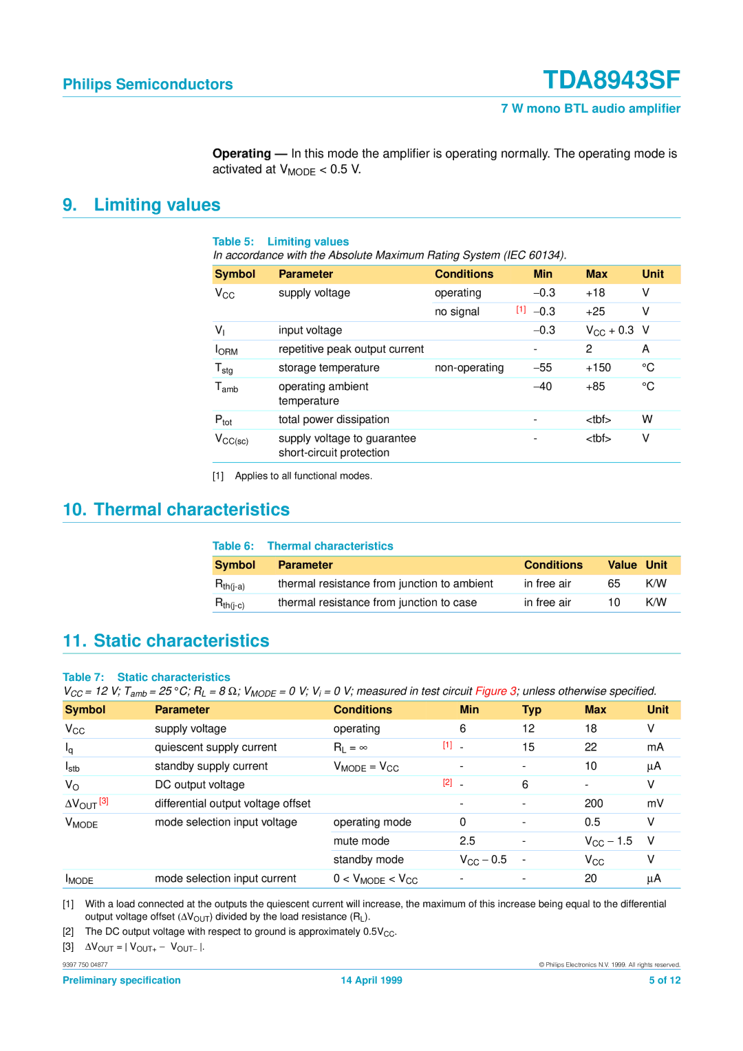
Table 5: | Limiting values |
|
|
|
|
In accordance with the Absolute Maximum Rating System (IEC 60134). |
|
| |||
|
|
|
|
|
|
Symbol | Parameter | Conditions | Min | Max | Unit |
VCC | supply voltage | operating | −0.3 | +18 | V |
|
| no signal | [1] −0.3 | +25 | V |
VI | input voltage |
| −0.3 | VCC + 0.3 | V |
IORM | repetitive peak output current |
| - | 2 | A |
Tstg | storage temperature | −55 | +150 | °C | |
Tamb | operating ambient |
| −40 | +85 | °C |
| temperature |
|
|
|
|
|
|
|
|
|
|
Ptot | total power dissipation |
| - | <tbf> | W |
VCC(sc) | supply voltage to guarantee |
| - | <tbf> | V |
|
|
|
|
| |
|
|
|
|
|
|
[1]Applies to all functional modes.
10.Thermal characteristics
Table 6: | Thermal characteristics |
|
|
|
Symbol | Parameter | Conditions | Value | Unit |
thermal resistance from junction to ambient | in free air | 65 | K/W | |
thermal resistance from junction to case | in free air | 10 | K/W |
11. Static characteristics
Table 7: Static characteristics
VCC = 12 V; Tamb = 25 °C; RL = 8 Ω; VMODE = 0 V; Vi = 0 V; measured in test circuit Figure 3; unless otherwise specified.
Symbol | Parameter | Conditions |
| Min | Typ | Max | Unit |
VCC | supply voltage | operating |
| 6 | 12 | 18 | V |
Iq | quiescent supply current | RL = ∞ | [1] | - | 15 | 22 | mA |
Istb | standby supply current | VMODE = VCC |
| - | - | 10 | μA |
V | DC output voltage |
| [2] | - | 6 | - | V |
O |
|
|
|
|
|
|
|
ΔVOUT [3] | differential output voltage offset |
|
| - | - | 200 | mV |
VMODE | mode selection input voltage | operating mode |
| 0 | - | 0.5 | V |
|
| mute mode |
| 2.5 | - | VCC − 1.5 | V |
|
| standby mode |
| VCC − 0.5 | - | VCC | V |
IMODE | mode selection input current | 0 < VMODE < VCC |
| - | - | 20 | μA |
[1]With a load connected at the outputs the quiescent current will increase, the maximum of this increase being equal to the differential output voltage offset (ΔVOUT) divided by the load resistance (RL).
[2]The DC output voltage with respect to ground is approximately 0.5VCC.
[3]ΔVOUT = VOUT+ − VOUT− .
9397 750 04877 | © Philips Electronics N.V. 1999. All rights reserved. |
Preliminary specification | 14 April 1999 | 5 of 12 |
