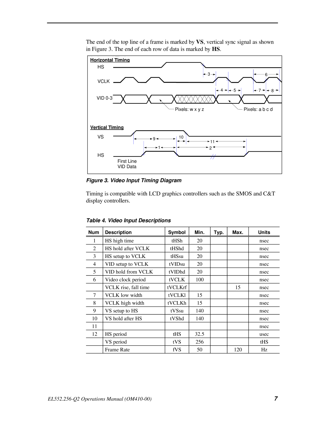
The end of the top line of a frame is marked by VS, vertical sync signal as shown in Figure 3. The end of each row of data is marked by HS.
Horizontal Timing |
|
|
|
|
|
HS |
|
|
|
|
|
|
| 3 |
|
| 6 |
VCLK |
|
|
|
|
|
|
| 4 | 5 | 7 | 8 |
VID |
|
|
|
|
|
|
| Pixels: w x y z |
| Pixels: a b c d | |
Vertical Timing |
|
|
|
|
|
VS | 9 | 10 |
|
|
|
| 11 |
|
|
| |
|
|
|
|
| |
| 1 | 2 |
|
|
|
HS |
|
|
|
|
|
First Line |
|
|
|
|
|
VID Data |
|
|
|
|
|
Figure 3. Video Input Timing Diagram
Timing is compatible with LCD graphics controllers such as the SMOS and C&T display controllers.
Table 4. Video Input Descriptions
Num | Description | Symbol | Min. | Typ. | Max. | Units |
|
|
|
|
|
|
|
1 | HS high time | tHSh | 20 |
|
| nsec |
2 | HS hold after VCLK | tHShd | 20 |
|
| nsec |
|
|
|
|
|
|
|
3 | HS setup to VCLK | tHSsu | 20 |
|
| nsec |
|
|
|
|
|
|
|
4 | VID setup to VCLK | tVIDsu | 20 |
|
| nsec |
|
|
|
|
|
|
|
5 | VID hold from VCLK | tVIDhd | 20 |
|
| nsec |
|
|
|
|
|
|
|
6 | Video clock period | tVCLK | 100 |
|
| nsec |
|
|
|
|
|
|
|
| VCLK rise, fall time | tVCLKrf |
|
| 15 | nsec |
|
|
|
|
|
|
|
7 | VCLK low width | tVCLKl | 15 |
|
| nsec |
|
|
|
|
|
|
|
8 | VCLK high width | tVCLKh | 15 |
|
| nsec |
|
|
|
|
|
|
|
9 | VS setup to HS | tVSsu | 140 |
|
| nsec |
|
|
|
|
|
|
|
10 | VS hold after HS | tVShd | 140 |
|
| nsec |
|
|
|
|
|
|
|
11 |
|
|
|
|
| nsec |
12 | HS period | tHS | 32.5 |
|
| usec |
|
|
|
|
|
|
|
| VS period | tVS | 256 |
|
| tHS |
| Frame Rate | fVS | 50 |
| 120 | Hz |
|
|
|
|
|
|
|
7 |
