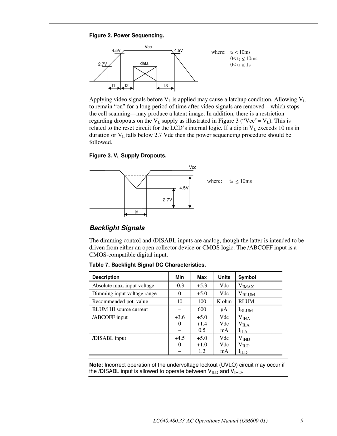
Figure 2. Power Sequencing.
Vcc
4.5V
2.7V | data |
4.5V | where: t1 ≤ 10ms | ||
|
| ||
|
| 0< t2 | ≤ 10ms |
|
| 0< t3 | ≤ 1s |
|
|
|
|
t1
t2
t3
Applying video signals before VL is applied may cause a latchup condition. Allowing VL to remain “on” for a long period of time after video signals are
Figure 3. VL Supply Dropouts.
Vcc
4.5V
where: td ≤ 10ms
2.7V
td
Backlight Signals
The dimming control and /DISABL inputs are analog, though the latter is intended to be driven from either an open collector device or CMOS logic. The /ABCOFF input is a
Table 7. Backlight Signal DC Characteristics.
| Description | Min | Max | Units | Symbol |
|
|
|
|
|
|
|
|
| Absolute max. input voltage | +5.3 | Vdc | VIMAX |
| |
| Dimming input voltage range | 0 | +5.0 | Vdc | VRLUM |
|
| Recommended pot. value | 10 | 100 | K ohm | RLUM |
|
| RLUM HI source current | – | 600 | µA | IRLUM |
|
| /ABCOFF input | +3.6 | +5.0 | Vdc | VIHA |
|
|
| 0 | +1.4 | Vdc | VILA |
|
|
| – | 0.5 | mA | IILA |
|
| /DISABL input | +4.5 | +5.0 | Vdc | VIHD |
|
|
| 0 | +1.0 | Vdc | VILD |
|
|
| – | 1.3 | mA | IILD |
|
|
|
|
|
|
|
|
Note: Incorrect operation of the undervoltage lockout (UVLO) circuit may occur if the /DISABL input is allowed to operate between VILD and VIHD.
9 |