EVALUATION BOARD MANUAL | S3F401F_BD_UM_REV1.00 |
|
|
3.2 JUMPER CONNECTION (Continued)
JP# |
| Description |
|
|
|
|
| Default Setting | ||||
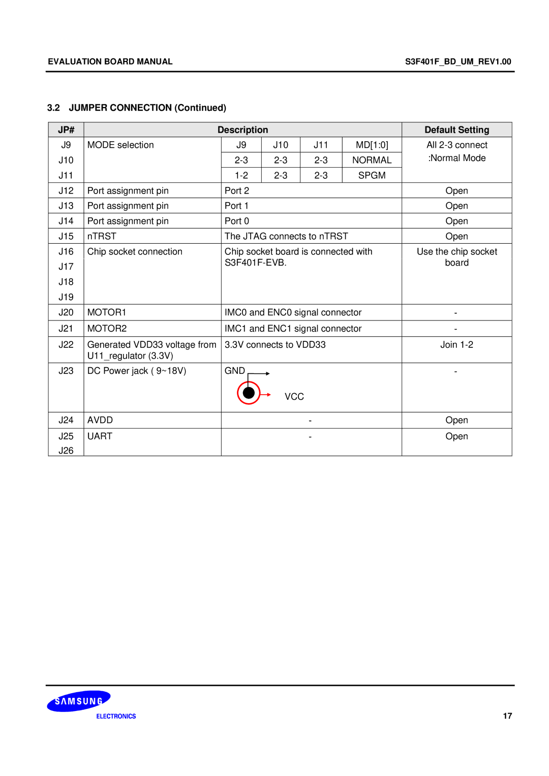
J9 | MODE selection |
| J9 |
| J10 |
| J11 |
| MD[1:0] | All | ||
J10 |
|
|
|
|
|
| NORMAL | :Normal Mode | ||||
J11 |
|
|
|
|
|
| SPGM |
| ||||
J12 | Port assignment pin |
| Port 2 |
|
|
|
|
| Open | |||
J13 | Port assignment pin |
| Port 1 |
|
|
|
|
| Open | |||
J14 | Port assignment pin |
| Port 0 |
|
|
|
|
| Open | |||
J15 | nTRST |
| The JTAG connects to nTRST |
| Open | |||||||
J16 | Chip socket connection |
| Chip socket board is connected with | Use the chip socket | ||||||||
J17 |
|
|
|
|
| board | ||||||
|
|
|
|
|
|
|
|
|
|
|
| |
J18 |
|
|
|
|
|
|
|
|
|
|
|
|
J19 |
|
|
|
|
|
|
|
|
|
|
|
|
J20 | MOTOR1 |
| IMC0 and ENC0 signal connector | - | ||||||||
|
|
|
|
|
|
| ||||||
J21 | MOTOR2 |
| IMC1 and ENC1 signal connector | - | ||||||||
|
|
|
|
|
|
|
| |||||
J22 | Generated VDD33 voltage from |
| 3.3V connects to VDD33 |
| Join | |||||||
| U11_regulator (3.3V) |
|
|
|
|
|
|
|
|
|
|
|
J23 | DC Power jack ( 9~18V) |
| GND |
|
| VCC |
|
|
| - | ||
|
|
|
|
| ||||||||
|
|
|
|
|
|
|
|
|
|
| ||
|
|
|
|
|
|
|
|
|
|
| ||
|
|
|
|
|
|
|
|
|
|
|
|
|
J24 | AVDD |
|
|
|
|
|
|
| - |
|
| Open |
|
|
|
|
|
|
|
|
|
|
|
|
|
J25 | UART |
|
|
|
|
|
|
| - |
|
| Open |
J26 |
|
|
|
|
|
|
|
|
|
|
|
|
17
