EVALUATION BOARD MANUAL | S3F401F_BD_UM_REV1.00 |
|
|
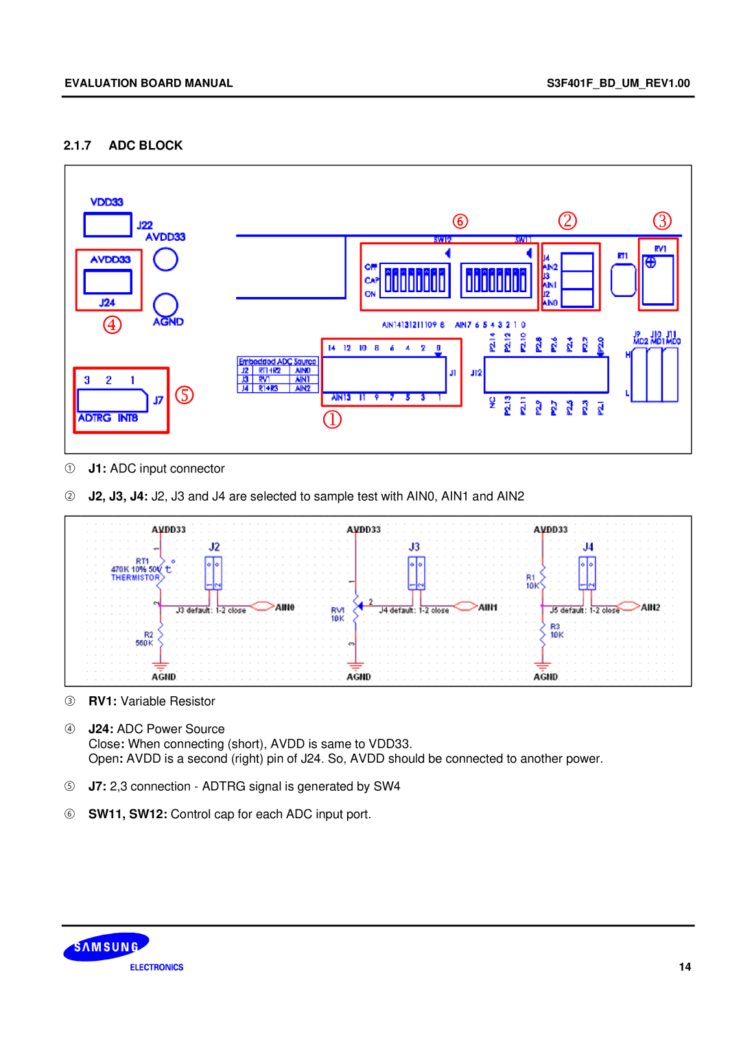
2.1.7ADC BLOCK
⑥ 2 3
4
5
1
①J1: ADC input connector
②J2, J3, J4: J2, J3 and J4 are selected to sample test with AIN0, AIN1 and AIN2
③RV1: Variable Resistor
④J24: ADC Power Source
Close: When connecting (short), AVDD is same to VDD33.
Open: AVDD is a second (right) pin of J24. So, AVDD should be connected to another power.
⑤J7: 2,3 connection - ADTRG signal is generated by SW4
⑥SW11, SW12: Control cap for each ADC input port.
14