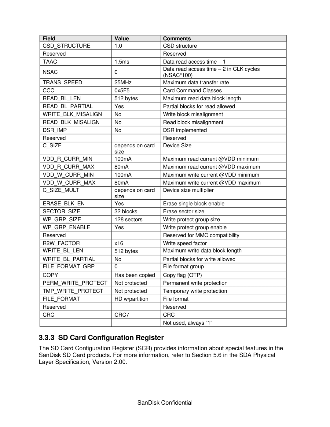
| Field | Value |
|
| Comments |
| CSD_STRUCTURE | 1.0 |
|
| CSD structure |
| Reserved |
|
|
| Reserved |
| TAAC | 1.5ms |
| Data read access time – 1 | |
| NSAC | 0 |
|
| Data read access time – 2 in CLK cycles |
|
|
| (NSAC*100) | ||
|
|
|
|
| |
| TRANS_SPEED | 25MHz | Maximum data transfer rate | ||
| CCC | 0x5F5 |
| Card Command Classes | |
| READ_BL_LEN | 512 bytes |
| Maximum read data block length | |
| READ_BL_PARTIAL | Yes |
| Partial blocks for read allowed | |
| WRITE_BLK_MISALIGN | No | Write block misalignment | ||
| READ_BLK_MISALIGN | No |
| Read block misalignment | |
| DSR_IMP | No |
| DSR implemented | |
| Reserved |
|
| Reserved | |
| C_SIZE | depends on card |
| Device Size | |
|
| size |
|
| |
| VDD_R_CURR_MIN | 100mA | Maximum read current @VDD minimum | ||
| VDD_R_CURR_MAX | 80mA |
| Maximum read current @VDD maximum | |
| VDD_W_CURR_MIN | 100mA |
| Maximum write current @VDD minimum | |
| VDD_W_CURR_MAX | 80mA |
| Maximum write current @VDD maximum | |
| C_SIZE_MULT | depends on card |
| Device size multiplier | |
|
| size |
|
| |
| ERASE_BLK_EN | Yes |
| Erase single block enable | |
| SECTOR_SIZE | 32 blocks |
| Erase sector size | |
| WP_GRP_SIZE | 128 sectors |
| Write protect group size | |
| WP_GRP_ENABLE | Yes |
| Write protect group enable | |
| Reserved |
|
| Reserved for MMC compatibility | |
| R2W_FACTOR | x16 | Write speed factor | ||
| WRITE_BL_LEN | 512 bytes |
| Maximum write data block length | |
| WRITE_BL_PARTIAL | No |
| Partial blocks for write allowed | |
| FILE_FORMAT_GRP | 0 |
| File format group | |
| COPY | Has been copied | Copy flag (OTP) | ||
| PERM_WRITE_PROTECT | Not protected |
| Permanent write protection | |
| TMP_WRITE_PROTECT | Not protected | Temporary write protection | ||
| FILE_FORMAT | HD w/partition | File format | ||
| Reserved |
|
| Reserved | |
| CRC | CRC7 | CRC | ||
|
|
|
|
| Not used, always “1” |
3.3.3 SD Card Configuration Register
The SD Card Configuration Register (SCR) provides information about special features in the SanDisk SD Card products. For more information, refer to Section 5.6 in the SDA Physical Layer Specification, Version 2.00.