Overview
Features
Revision History
Updated
Document No Release Date Changes
Added
Table of Contents
Common Memory Description and Operation
Attribute Memory Description and Operation
Space Description and Operation
ATA and True IDE Register Decoding
ATA Command Set
Related Documentation
Sales and Support Part Numbering
List of Figures
List of Tables
SSD-CXXXI-3600 Data Sheet
Part Numbering Nomenclature
Physical Dimensions
Physical Specifications
System Performance
Product Specifications
System Power Requirements
Operational Life Span
SiliconDrive Part# Capacity Service Life GB Written per Day
Reliability
Product Capacity Number Bytes Sectors Cylinders Heads Track
Product Capacity Specifications
Environmental Specifications
Pin Assignments
Electrical Specification
Signal Name Pin Type Description
Signal Descriptions
Dasp
Spkr
Inpack
Csel
Dmarq
True IDE mode
GND
Ground
Iowr
This signal is not used in this mode PC Card memory Mode
Iord
Ireq
ATA SEL
RDY/-BSY
+5V, +3.3V power PC Card memory Mode
Reset
REG
Dmack
Voltage Sense Signals
This signal is the same for all modes PC Card I/O Mode
Wait
Iordy
Absolute Maximum Ratings
Symbol Parameter Minimum Maximum Units
IOIS16
DC Characteristics
Symbol Parameter Maximum Units
Symbol Parameter V ±10% 5V ±10% Units Minimum Maximum
Capacitance
Attribute and Common Memory Read Timing
Attribute and Common Memory Read Timing
Attribute and Common Memory Write Timing
Attribute and Common Memory Write Timing
O Access Read Timing
Access Read Timing
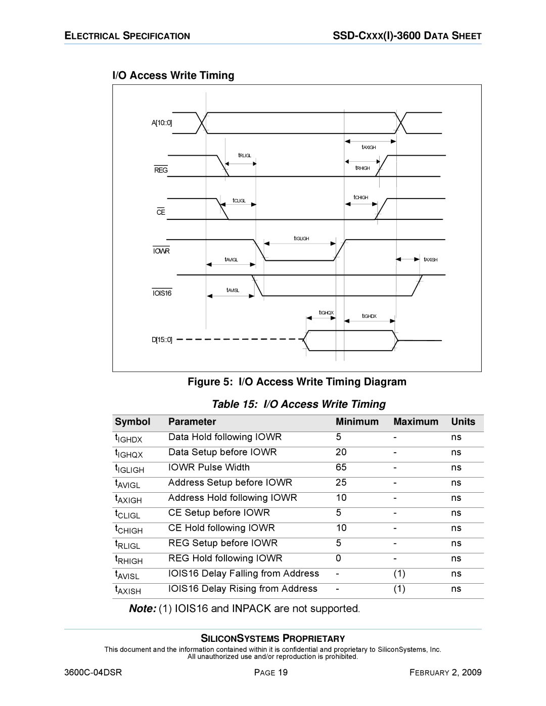
O Access Write Timing
Access Write Timing
True IDE Read/Write Access Timing
True IDE Read/Write Access Timing
True IDE Multiword DMA Read/Write Access Timing
True IDE Multiword DMA Read/Write Access Timing
Attribute Memory Description and Operation
D158 D70 Mode
Attribute Memory Read Operations
Function REG# CE1# CE2#
Attribute Memory Write Operations
Register Operation Addr CE1#
Attribute Memory Map
Card Information Structure
Attribute Data Description of Contents CIS Function Offset
Cistplfunce
Tpcemi
Tpcefs
Tpceio
Exponent Nominal voltage = VCC nominal value A6h 1Eh
IRQ
Configuration table entry tuple Tuple code E4h 12h
Exponent Nominal voltage = VCC nominal value F0h 4Dh
SSD-CXXXI-3600 Data Sheet
Card Information Structure
Bits Description
Configuration Option Register 200h
Sreset
Read Changed SigChg IOis8 PwrDn Int Write Default Value
Configuration and Status Register 202h
Rrdy
Pin Placement Register 204h
Crdy
Socket and Copy Register 206h
Copy Number Socket Number Default Value
Read/Write
RFU
Common Memory Write Operations
Common Memory Description and Operation
Common Memory Read Operations
Space Description and Operation
Function Mode REG# CE1# CE2# A0 IORD# IOWR# D158 D70
O Space Read Operations
O Space Write Operations
Reg# Offset A10 A9A4 OE# = L WE# = L
ATA and True IDE Register Decoding
Memory-Mapped Register Decoding
Independent I/O Mode Register Decoding
Primary Secondary
Primary and Secondary I/O Mapped Register Decoding
Reg# A10 A9A4
CS0# CS1# DA02 DA01 DA00
Task File Register Specification
Track 0 Not Found TKONF. Set when the execute drive
Error Register
ATA Registers
Media Changed MC. Set to
Operation
Feature Register
Read/Write
Byte
Sector Count Register
Read/Write Sector Count Default Value
Logical Block Number bits A07-A00 LBA Addressing
Sector Number Register
Logical Block Number bits A15-A08 LBA Addressing
Cylinder Low Register
Logical Block Number bits A23-A16 LBA Addressing
Cylinder High Register
LBA27 LBA26 LBA25 LBA24
Drive/Head Register
HS3 HS2 HS1 HS0
Status Register
Drive Write Fault DWF. Always set to
BSY Drdy
DRQ Corr IDX ERR
Operation Read/Write ATA Command Code
Command Register
Alternate Status Register
NIEN
Device Control Register
Srst
Device Address Register
Read/Write NWTG NHS3 NHS2 NHS1 NHS0 NDS1 NDS0 Default Value
ATA Command Block and Set Description
ATA Command Block and SET Description
ATA Command Set
Class Command Name Registers Used Code
ATA Command Set
Register
Check Power Mode 98h, E5h
Check Power Mode 98h, E5h
Executive Drive Diagnostic 90h
Executive Drive Diagnostic 90h
Format Track 50h
Drive Head Number LBA27-24 Command 50h
Format Track 50h
Identify Drive ECh
Identify Drive ECh
Identify Drive Drive Attribute Data
Word Data Default Bytes Data Description Address
044Ah fixed
ID bit in IDE
Word Data Default Bytes Data Description Address
Identify Drive Drive Attribute Data
Idle 97h, E3h
Idle 97h, E3h
Idle Immediate 95h, E1h
Idle Immediate 95h, E1h
Initialize Drive Parameters 91h
Initialize Drive Parameters 91h
Recalibrate 1Xh
Drive Command 1Xh
Recalibrate 1Xh
Read Buffer E4h
Read Buffer E4h
Read DMA C8h
Drive Head Number LBA27-24 Command C8h
Read DMA C8h
LBA
Read Multiple C4h
Drive Head Number LBA27-24 Command C4h
Read Multiple C4h
Read Sector 20h, 21h
Drive Head Number LBA27-24 Command 20h or 21h
Read Sector 20h, 21h
Read Long Sectors 22h, 23h
Drive Head Number LBA27-24 Command 22h or 23h
Read Long Sectors 22h, 23h
Read Verify Sectors 40h, 41h
Drive Head Number LBA27-24 Command 40h or 41h
Read Verify Sectors 40h, 41h
Seek 7Xh
Drive Head Number LBA27-24 Command 7Xh
Seek 7Xh
Set Features EFh
Set Features EFh
Set Features’ Attributes
Feature Operation
Set Multiple Mode C6h
Set Multiple Mode C6h
Set Sleep Mode 99h, E6h
Set Sleep Mode 99h, E6h
Standby 96h, E2h
Standby 96h, E2h
Standby Immediate 94h, E0h
Standby Immediate 94h, E0h
Write Buffer E8h
Write Buffer E8h
Write DMA CAh
Drive Head NumberLBA27-24 Command CAh
Write DMA CAh
Write Multiple C5h
Drive Head NumberLBA27-24 Command C5h
Write Multiple C5h
Write Sectors 30h, 31h
Drive Head Number LBA27-24 Command 30h or 31h
Write Sectors 30h, 31h
Write Long Sectors 32h, 33h
Drive Head Number LBA27-24 Command 32h or 33h
Write Long Sectors 32h, 33h
Erase Sectors C0h
Drive Head Number LBA27-24 Command C0h
Erase Sectors C0h
Extended Error Codes Description
Extended Error Codes
Request Sense 03h
Request Sense 03h
Translate Sector 87h
Drive Head Number LBA27-24 Command 87h
Translate Sector 87h
Wear-Level F5h
Wear-Level F5h
Write Multiple w/o Erase CDh
Drive Head Number LBA27-24 Command CDh
Write Multiple w/o Erase CDh
Write Sectors w/o Erase 38h
Drive Head Number LBA27-24 Command 38h
Write Sectors w/o Erase 38h
Write Verify 3Ch
Drive Head Number LBA27-24 Command 3Ch
Write Verify 3Ch
Part Numbering
Sales and Support
Part Numbering Nomenclature
Part Numbers
Sample Label
Front Label Standard Back Label with Lot Code Information
Related Documentation
Related Documentation