CP2112-EK
5. Target Board
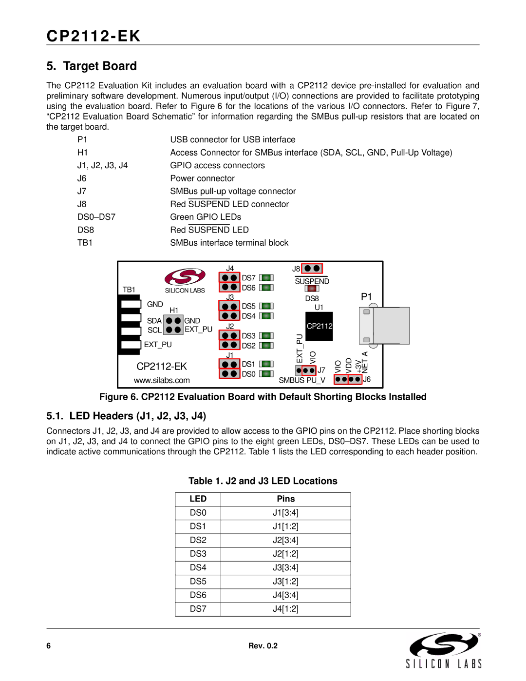
The CP2112 Evaluation Kit includes an evaluation board with a CP2112 device
P1 | USB connector for USB interface | |||
H1 | Access Connector for SMBus interface (SDA, SCL, GND, | |||
J1, J2, J3, J4 | GPIO access connectors | |||
J6 | Power connector | |||
J7 | SMBus | |||
J8 | Red |
|
| LED connector |
SUSPEND | ||||
Green GPIO LEDs | ||||
DS8 | Red |
| LED | |
SUSPEND | ||||
TB1 | SMBus interface terminal block | |||
TB1 | SILICON LABS |
GND H1
SDA ![]()
![]() GND
GND
![]() SCL
SCL ![]()
![]() EXT_PU
EXT_PU ![]() EXT_PU
EXT_PU
www.silabs.com
J4
![]()
![]()
![]()
![]() DS7
DS7 ![]()
![]()
![]()
![]()
![]()
![]() DS6
DS6 ![]() J3
J3
![]()
![]()
![]()
![]() DS5
DS5 ![]()
![]()
![]() DS4
DS4 ![]()
![]()
![]()
![]()
J2
![]()
![]()
![]()
![]() DS3
DS3 ![]()
![]()
![]()
![]()
![]()
![]() DS2
DS2 ![]() J1
J1
![]()
![]()
![]()
![]() DS1
DS1 ![]()
![]()
![]() DS0
DS0 ![]()
![]()
![]()
![]()
J8 |
|
SUSPEND |
|
DS8 | P1 |
U1 |
|
CP2112 |
|
EXTPU VIOJ7 | VIO VDD +3V NET A |
SMBUS PU_V | J6 |
Figure 6. CP2112 Evaluation Board with Default Shorting Blocks Installed
5.1. LED Headers (J1, J2, J3, J4)
Connectors J1, J2, J3, and J4 are provided to allow access to the GPIO pins on the CP2112. Place shorting blocks on J1, J2, J3, and J4 to connect the GPIO pins to the eight green LEDs,
Table 1. J2 and J3 LED Locations
| LED | Pins |
|
|
|
|
|
| DS0 | J1[3:4] |
|
|
|
|
|
| DS1 | J1[1:2] |
|
|
|
|
|
| DS2 | J2[3:4] |
|
|
|
|
|
| DS3 | J2[1:2] |
|
|
|
|
|
| DS4 | J3[3:4] |
|
|
|
|
|
| DS5 | J3[1:2] |
|
|
|
|
|
| DS6 | J4[3:4] |
|
|
|
|
|
| DS7 | J4[1:2] |
|
|
|
|
|
|
|
|
|
6 | Rev. 0.2 |