Si85xx-TB UG
4. Si85xx Evaluation Board
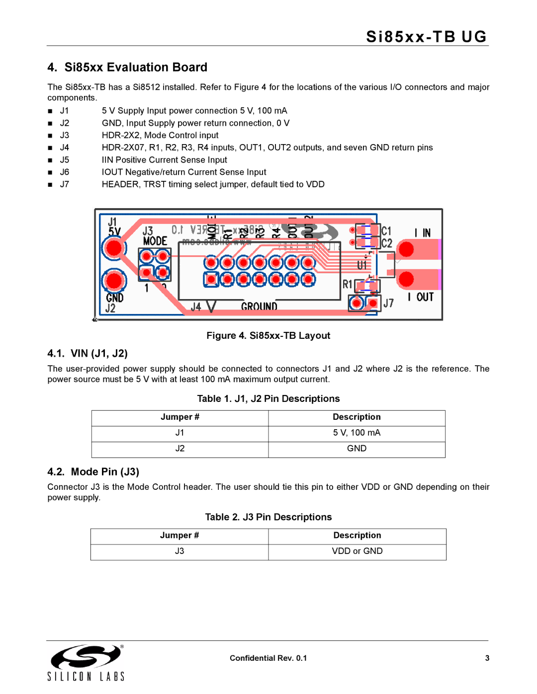
The
| J1 | 5 V Supply Input power connection 5 V, 100 mA |
| J2 | GND, Input Supply power return connection, 0 V |
J3
J4
| J5 | IIN Positive Current Sense Input |
| J6 | IOUT Negative/return Current Sense Input |
| J7 | HEADER, TRST timing select jumper, default tied to VDD |
Figure 4. Si85xx-TB Layout
4.1. VIN (J1, J2)
The
Table 1. J1, J2 Pin Descriptions
Jumper # | Description |
|
|
J1 | 5 V, 100 mA |
|
|
J2 | GND |
|
|
4.2. Mode Pin (J3)
Connector J3 is the Mode Control header. The user should tie this pin to either VDD or GND depending on their power supply.
| Table 2. J3 Pin Descriptions | |
|
|
|
Jumper # |
| Description |
|
|
|
J3 |
| VDD or GND |
|
|
|
Confidential Rev. 0.1 | 3 |