SECTION 6
DIAGRAMS
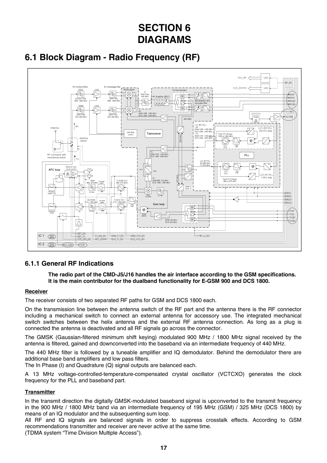
6.1 Block Diagram - Radio Frequency (RF)
|
| Rx frontend filter |
| Rx interstage filter |
|
|
|
|
|
|
|
|
| ||
|
| DCS | LNA |
| 1st Rx mixer | IF |
|
| IQ Demodulator |
|
| ||||
|
|
|
|
|
|
|
|
|
|
|
|
|
|
| |
|
|
|
|
|
| RF | IF | SAW Filter |
|
|
|
|
|
|
|
|
| Ceramic Filter |
|
| SAW Filter |
| 440 MHz |
| IF Amplifier (PGC) |
|
| I |
|
| |
|
|
|
| LO |
|
|
|
|
|
|
| BB amplifier and | |||
|
| 1805..1880 MHz |
|
| 1805..1880 MHz |
|
|
|
| 90° |
|
| |||
|
|
|
|
|
|
|
| ∑ | 0 |
| |||||
|
|
|
|
|
|
|
|
|
|
|
|
| low pass filter | ||
|
| GSM | LNA |
|
|
|
|
|
|
|
| ° |
| ||
|
|
|
|
|
|
|
|
|
|
|
|
| |||
|
|
|
|
|
|
|
|
|
|
|
|
| Q |
|
|
|
|
|
|
|
| RF | IF | RX: |
|
|
|
|
|
|
|
|
|
|
|
|
|
|
|
|
|
|
|
|
|
| |
|
| SAW Filter |
|
| SAW Filter |
| GSM 1365..1400 MHz |
|
|
|
|
| |||
|
|
|
| LO | DCS 1365..1440 MHz |
|
|
|
|
| |||||
|
| 925..960 MHz |
|
| 925..960 MHz |
|
|
|
|
| |||||
|
|
|
|
|
|
|
|
|
| 440 MHz |
| ||||
|
|
|
|
|
|
|
|
|
|
|
|
|
| ||
|
| RX |
|
|
|
|
|
|
|
|
|
|
|
| LO1 (RF) PLL: |
| Antenna |
|
|
|
|
|
|
|
| 1 |
|
|
| - RX - | |
|
|
|
|
|
|
|
|
|
|
|
|
| |||
|
|
|
|
|
|
|
|
|
|
|
|
|
|
| GSM 1365..1400 MHz |
|
|
|
|
|
| LNA Bias | Transceiver |
| 2 |
|
| DCS 1365..1440 MHz | |||
|
|
|
|
|
|
|
|
|
| - TX - | |||||
|
|
|
|
|
|
| control |
| MHz |
|
| ||||
|
| Antenna |
|
|
|
|
|
|
|
|
|
| GSM 1370..1440 MHz | ||
|
|
|
|
|
|
|
|
|
| 880 |
|
| DCS 1385..1460 MHz | ||
|
|
| Switch |
|
|
|
|
|
|
|
|
|
|
| |
|
|
|
|
|
|
|
|
| TX: |
|
|
|
|
| |
| RF Connector with |
|
|
|
|
|
| GSM 1370..1440 MHz |
|
|
|
|
| ||
| mechanical switch |
|
|
|
|
|
| DCS 1385..1460 MHz |
|
|
|
|
| ||
|
| TX |
|
|
|
|
|
|
|
|
|
|
|
| LO2 (IF) PLL |
|
|
|
|
|
|
|
|
|
|
|
|
|
|
| |
|
|
|
|
|
|
|
|
|
|
|
|
|
|
| RX 880 MHz |
|
| Detector and |
|
|
|
|
|
|
|
|
|
|
|
| TX 975 MHz |
|
|
|
|
|
|
| 2 |
|
|
|
|
|
|
| |
| APC loop | Level control |
|
|
|
|
|
|
|
|
|
|
|
| |
|
|
|
|
|
| DCS |
| GSM |
|
|
|
|
| ||
|
|
|
|
|
|
|
| 1 |
|
|
|
|
|
| |
|
|
|
|
|
|
|
|
|
|
| MHz |
| 5 |
|
|
|
|
|
|
|
|
|
|
|
| TX: |
|
| 1 |
| |
|
|
| GSM | Pin diode | Tx GSM VCO |
|
|
| GSM 685..720 MHz | 975 |
|
|
|
| |
|
|
| 880..915 MHz | switch | 880..915 MHz |
|
|
| DCS 1385..1460 MHz |
|
|
|
|
| |
|
|
|
|
|
|
|
|
|
|
| 3/5 | GSM :5 |
| ||
|
|
|
|
|
|
|
|
|
|
|
|
|
| ||
|
|
|
|
|
|
|
|
|
|
|
| 1 | DCS :3 |
| |
| Directional | PA | LP Filter |
|
|
|
|
|
|
|
|
|
|
|
|
| coupler + LPF |
|
|
|
|
|
| Down |
|
|
|
|
|
|
|
|
|
|
|
|
|
|
|
| LP Filter |
|
|
|
|
| |
|
|
|
|
|
|
|
| Converter |
|
|
|
|
|
| |
|
|
| DCS1800 | Pin diode | Tx DCS VCO |
|
|
|
|
|
|
|
|
| |
|
|
| 1710..1785 MHz | switch | 1710..1785 MHz |
|
|
| Sum loop |
|
|
|
|
| |
|
|
|
|
|
|
| Loop |
|
|
|
|
|
|
| |
|
|
|
|
|
|
| Filter | ϕ |
|
|
|
|
|
| I |
|
|
|
|
|
|
|
|
|
|
|
|
|
| ||
| Directional | PA | LP Filter |
|
|
|
|
|
|
|
|
| ∑ | 90° | 0 |
| coupler |
|
|
|
|
|
| Phase |
|
|
|
|
| ||
|
|
|
|
|
|
|
|
|
|
|
|
|
| ° | |
|
|
|
|
|
|
|
| detector |
|
|
|
|
|
| |
|
|
|
|
|
|
|
|
|
| GSM 195 MHz |
|
|
| Q | |
|
|
|
|
|
|
|
|
|
| DCS 325 MHz |
|
|
|
| |
IC 1 | Digital | DET_EN | TX_SW_EN | GSM_TX_EN | GSM_VCO_EN |
|
|
|
|
|
| RF_IC_EN | |||
DET_TX |
|
|
|
|
|
| |||||||||
| signals | TXP_OFS_EN | APC_DOWN | DCS_TX_EN | DCS_VCO_EN |
|
|
|
|
|
|
| |||
|
|
|
|
|
|
|
|
| |||||||
IC 2 | Analog | AUX_DAC | TXP |
|
|
|
|
|
|
|
|
|
|
|
|
signals |
|
|
|
|
|
|
|
|
|
|
|
| |||
VCC_RF ![]() LDO
LDO ![]()
RF_EN
VCC_SYNTH ![]() LDO
LDO ![]()
![]() RXIP
RXIP
![]() RXIN
RXIN
![]() RXQP
RXQP
![]() RXQN
RXQN
VCTCXO | AFC |
| |
13 MHz | CLK13M |
NLO1 (RF) PLL
|
| N+1 | 200 kHz step |
Total VCO Range: |
| 1 |
|
|
|
| |
1365 to 1460 MHz |
| ϕ |
|
|
| N | |
|
|
| 1 |
LO1 | Loop |
|
|
VCO | Filter |
|
|
|
|
| |
|
| PLL |
|
|
| ϕ | N |
|
|
| 1 |
LO2 | Loop |
|
|
VCO | Filter | M | LO2 (IF) PLL |
| |||
|
|
| |
Total VCO Range: | 1 | 1 MHz step | |
|
| ||
880 to 975 MHz |
|
| |
SERCK
SERDA
SERLE1
SERLE2
TXIP
TXIN
TXQP
TXQN
6.1.1 General RF Indications
The radio part of the
Receiver
The receiver consists of two separated RF paths for GSM and DCS 1800 each.
On the transmission line between the antenna switch of the RF part and the antenna there is the RF connector including a mechanical switch to connect an external antenna for accessory use. The integrated mechanical switch switches between the helix antenna and the external RF antenna connection. As long as a plug is connected the antenna is deactivated and all RF signals go across the connector.
The GMSK
The 440 MHz filter is followed by a tuneable amplifier and IQ demodulator. Behind the demodulator there are additional base band amplifiers and low pass filters.
The In Phase (I) and Quadrature (Q) signal outputs are balanced each.
A13 MHz
Transmitter
In the transmit direction the digitally
All RF and IQ signals are balanced signals in order to suppress crosstalk effects. According to GSM recommendations transmitter and receiver are never active at the same time.
(TDMA system “Time Division Multiple Access”).
17