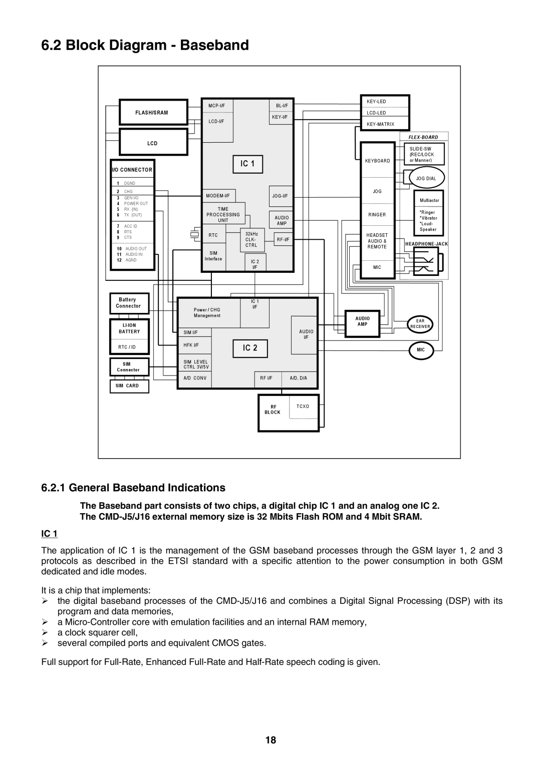
6.2 Block Diagram - Baseband
FLASH/SRAM
LCD
IC 1
I/O CONNECTOR
1DGND
2 | CHG |
|
|
| MODEM | |
|
| |||||
3 |
|
|
|
| ||
GEN I/O |
| |||||
|
|
| ||||
4POWER OUT
5 | RX (IN) | TIME |
|
| |
6 | TX (OUT) | PROCCESSING |
| AUDIO | |
|
| UNIT |
| ||
7 | ACC ID |
| AMP | ||
|
| ||||
|
|
| |||
8 | RTS | RTC | 32kHz |
| |
9 | CTS | ||||
| CLK- | ||||
10 | AUDIO OUT |
| CTRL |
| |
SIM |
|
| |||
11 | AUDIO IN |
|
| ||
12 | AGND | Interface | IC 2 |
| |
|
|
| I/F |
| |
Battery |
| IC 1 |
| ||
Connector | Power / CHG | I/F |
| ||
KEYBOARD
JOG
RINGER
HEADSET
AUDIO &
REMOTE
MIC
FLEX-BOARD
JOG DIAL
Multiactor
*Ringer
*Vibrator *Loud- Speaker
Management |
|
|
|
| ||
BATTERY |
|
| SIM I/F |
| AUDIO |
|
|
| |||
|
|
|
|
| I/F |
|
|
|
| ||
RTC / ID | HFK I/F | IC 2 |
|
SIM |
| SIM LEVEL |
| CTRL 3V/5V | |
Connector |
| |
|
|
A/D CONV | RF I/F | A/D, D/A |
SIM CARD |
RF ![]() TCXO
TCXO
BLOCK
AUDIO | EAR | |
AMP | ||
RECEIVER | ||
|
MIC
6.2.1 General Baseband Indications
The Baseband part consists of two chips, a digital chip IC 1 and an analog one IC 2. The
IC 1
The application of IC 1 is the management of the GSM baseband processes through the GSM layer 1, 2 and 3 protocols as described in the ETSI standard with a specific attention to the power consumption in both GSM dedicated and idle modes.
It is a chip that implements:
the digital baseband processes of the
a
several compiled ports and equivalent CMOS gates.
Full support for
18