SECTION 6
DIAGRAMS
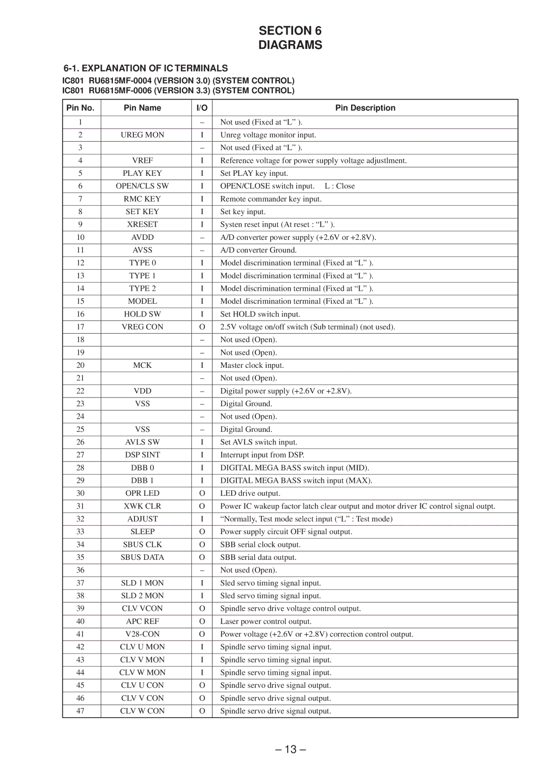
6-1. EXPLANATION OF IC TERMINALS
IC801
IC801
Pin No. | Pin Name | I/O | Pin Description |
|
|
|
|
1 |
| – | Not used (Fixed at “L” ). |
|
|
|
|
2 | UREG MON | I | Unreg voltage monitor input. |
|
|
|
|
3 |
| – | Not used (Fixed at “L” ). |
|
|
|
|
4 | VREF | I | Reference voltage for power supply voltage adjustlment. |
|
|
|
|
5 | PLAY KEY | I | Set PLAY key input. |
|
|
|
|
6 | OPEN/CLS SW | I | OPEN/CLOSE switch input. L : Close |
|
|
|
|
7 | RMC KEY | I | Remote commander key input. |
|
|
|
|
8 | SET KEY | I | Set key input. |
|
|
|
|
9 | XRESET | I | Systen reset input (At reset : “L” ). |
|
|
|
|
10 | AVDD | – | A/D converter power supply (+2.6V or +2.8V). |
|
|
|
|
11 | AVSS | – | A/D converter Ground. |
|
|
|
|
12 | TYPE 0 | I | Model discrimination terminal (Fixed at “L” ). |
|
|
|
|
13 | TYPE 1 | I | Model discrimination terminal (Fixed at “L” ). |
|
|
|
|
14 | TYPE 2 | I | Model discrimination terminal (Fixed at “L” ). |
|
|
|
|
15 | MODEL | I | Model discrimination terminal (Fixed at “L” ). |
|
|
|
|
16 | HOLD SW | I | Set HOLD switch input. |
|
|
|
|
17 | VREG CON | O | 2.5V voltage on/off switch (Sub terminal) (not used). |
|
|
|
|
18 |
| – | Not used (Open). |
|
|
|
|
19 |
| – | Not used (Open). |
|
|
|
|
20 | MCK | I | Master clock input. |
|
|
|
|
21 |
| – | Not used (Open). |
|
|
|
|
22 | VDD | – | Digital power supply (+2.6V or +2.8V). |
|
|
|
|
23 | VSS | – | Digital Ground. |
|
|
|
|
24 |
| – | Not used (Open). |
|
|
|
|
25 | VSS | – | Digital Ground. |
|
|
|
|
26 | AVLS SW | I | Set AVLS switch input. |
|
|
|
|
27 | DSP SINT | I | Interrupt input from DSP. |
|
|
|
|
28 | DBB 0 | I | DIGITAL MEGA BASS switch input (MID). |
|
|
|
|
29 | DBB 1 | I | DIGITAL MEGA BASS switch input (MAX). |
|
|
|
|
30 | OPR LED | O | LED drive output. |
|
|
|
|
31 | XWK CLR | O | Power IC wakeup factor latch clear output and motor driver IC control signal outpt. |
|
|
|
|
32 | ADJUST | I | “Normally, Test mode select input (“L” : Test mode) |
|
|
|
|
33 | SLEEP | O | Power supply circuit OFF signal output. |
|
|
|
|
34 | SBUS CLK | O | SBB serial clock output. |
|
|
|
|
35 | SBUS DATA | O | SBB serial data output. |
|
|
|
|
36 |
| – | Not used (Open). |
|
|
|
|
37 | SLD 1 MON | I | Sled servo timing signal input. |
|
|
|
|
38 | SLD 2 MON | I | Sled servo timing signal input. |
|
|
|
|
39 | CLV VCON | O | Spindle servo drive voltage control output. |
|
|
|
|
40 | APC REF | O | Laser power control output. |
|
|
|
|
41 |
| O | Power voltage (+2.6V or +2.8V) correction control output. |
|
|
|
|
42 | CLV U MON | I | Spindle servo timing signal input. |
|
|
|
|
43 | CLV V MON | I | Spindle servo timing signal input. |
|
|
|
|
44 | CLV W MON | I | Spindle servo timing signal input. |
|
|
|
|
45 | CLV U CON | O | Spindle servo drive signal output. |
|
|
|
|
46 | CLV V CON | O | Spindle servo drive signal output. |
|
|
|
|
47 | CLV W CON | O | Spindle servo drive signal output. |
|
|
|
|
– 13 –