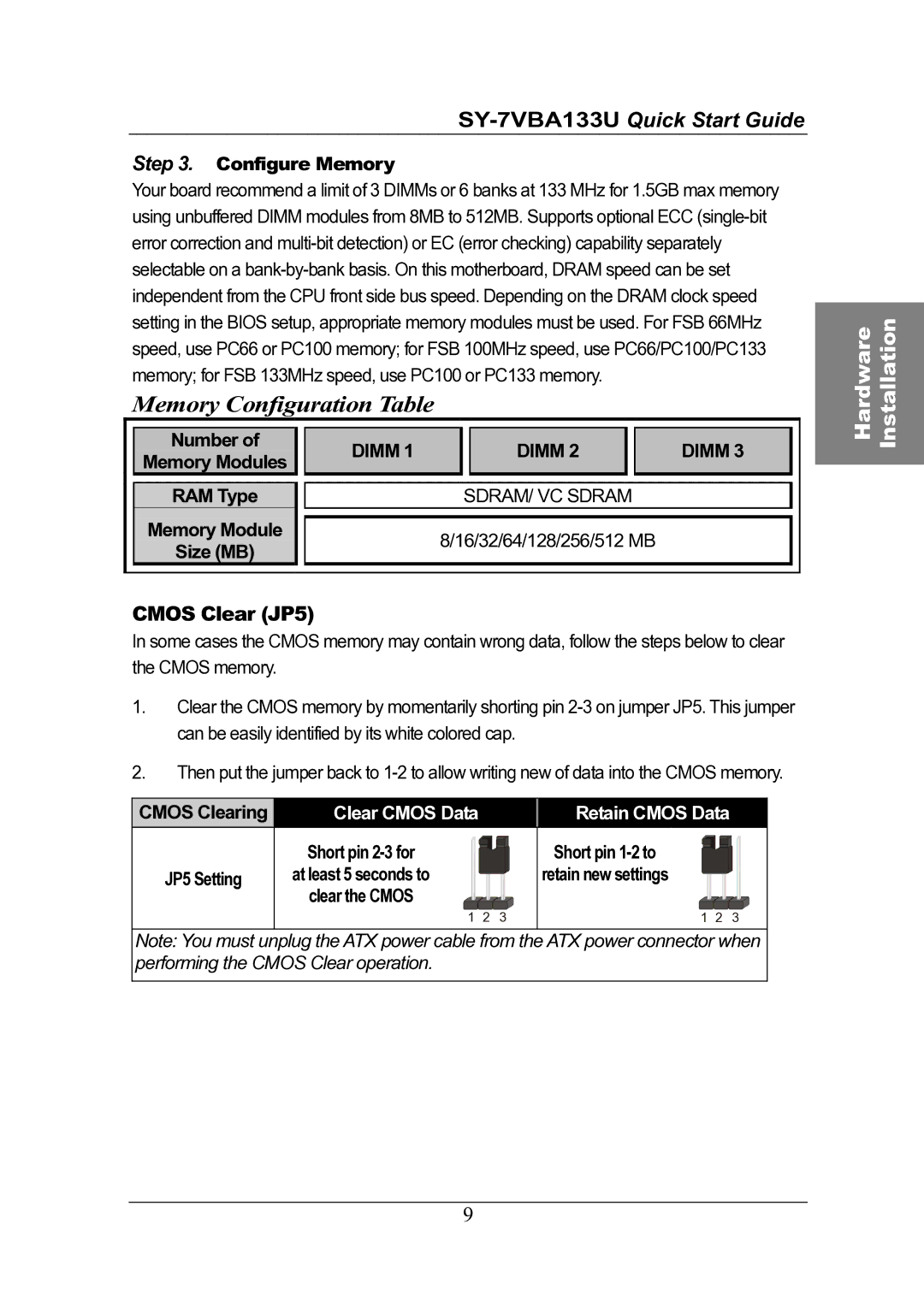
Step 3. Configure Memory
Your board recommend a limit of 3 DIMMs or 6 banks at 133 MHz for 1.5GB max memory using unbuffered DIMM modules from 8MB to 512MB. Supports optional ECC
Memory Configuration Table
|
|
|
|
|
|
|
|
|
|
|
| Number of |
| DIMM 1 |
|
| DIMM 2 |
|
| DIMM 3 |
|
| Memory Modules |
|
|
|
|
|
| |||
|
|
|
|
|
|
|
|
|
| |
|
|
|
|
|
|
|
| |||
| RAM Type |
|
|
| SDRAM/ VC SDRAM |
|
| |||
| Memory Module |
|
|
|
|
|
|
|
|
|
|
|
| 8/16/32/64/128/256/512 MB |
|
| |||||
| Size (MB) |
|
|
|
| |||||
|
|
|
|
|
|
|
|
|
| |
|
|
|
|
|
|
|
|
|
|
|
CMOS Clear (JP5)
In some cases the CMOS memory may contain wrong data, follow the steps below to clear the CMOS memory.
1.Clear the CMOS memory by momentarily shorting pin
2.Then put the jumper back to
CMOS Clearing | Clear CMOS Data |
|
| Retain CMOS Data |
| |
| Short pin |
|
| Short pin |
|
|
JP5 Setting | at least 5 seconds to |
|
| retain new settings |
|
|
| clear the CMOS |
|
|
|
|
|
| 1 | 2 | 3 | 1 | 2 | 3 |
Note: You must unplug the ATX power cable from the ATX power connector when performing the CMOS Clear operation.
Hardware Installation
9