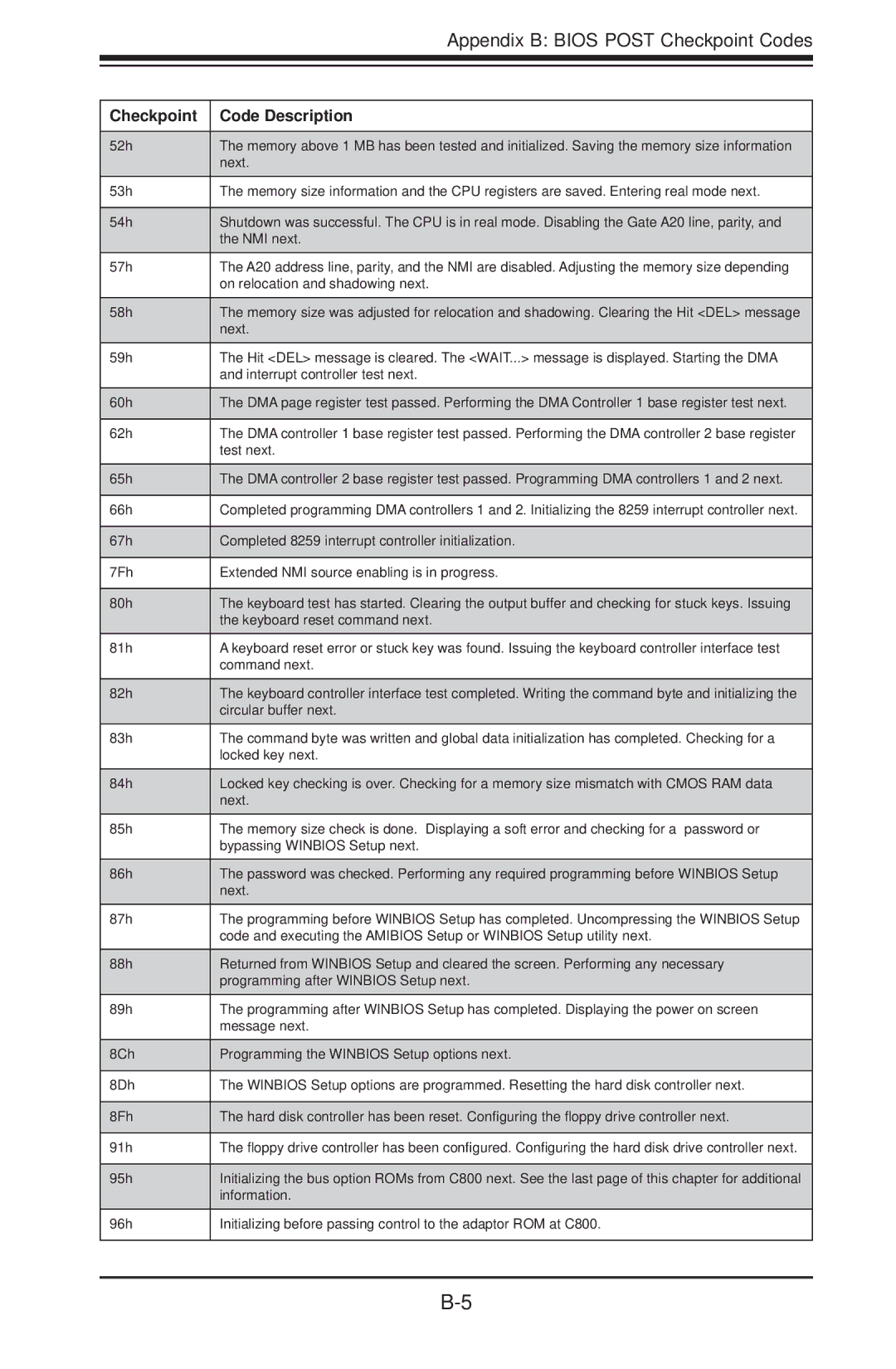
Appendix B: BIOS POST Checkpoint Codes


Checkpoint

Code Description


52h

The memory above 1 MB has been tested and initialized. Saving the memory size information


next.


53h

The memory size information and the CPU registers are saved. Entering real mode next.


54h

Shutdown was successful. The CPU is in real mode. Disabling the Gate A20 line, parity, and


the NMI next.


57h

The A20 address line, parity, and the NMI are disabled. Adjusting the memory size depending


on relocation and shadowing next.


58h

The memory size was adjusted for relocation and shadowing. Clearing the Hit <DEL> message


next.


59h

The Hit <DEL> message is cleared. The <WAIT...> message is displayed. Starting the DMA


and interrupt controller test next.


60h

The DMA page register test passed. Performing the DMA Controller 1 base register test next.


62h

The DMA controller 1 base register test passed. Performing the DMA controller 2 base register


test next.


65h

The DMA controller 2 base register test passed. Programming DMA controllers 1 and 2 next.


66h

Completed programming DMA controllers 1 and 2. Initializing the 8259 interrupt controller next.


67h

Completed 8259 interrupt controller initialization.


7Fh

Extended NMI source enabling is in progress.


80h

The keyboard test has started. Clearing the output buffer and checking for stuck keys. Issuing


the keyboard reset command next.


81h

A keyboard reset error or stuck key was found. Issuing the keyboard controller interface test


command next.


82h

The keyboard controller interface test completed. Writing the command byte and initializing the


circular buffer next.


83h

The command byte was written and global data initialization has completed. Checking for a


locked key next.


84h

Locked key checking is over. Checking for a memory size mismatch with CMOS RAM data


next.


85h

The memory size check is done. Displaying a soft error and checking for a password or


bypassing WINBIOS Setup next.


86h

The password was checked. Performing any required programming before WINBIOS Setup


next.


87h

The programming before WINBIOS Setup has completed. Uncompressing the WINBIOS Setup


code and executing the AMIBIOS Setup or WINBIOS Setup utility next.


88h

Returned from WINBIOS Setup and cleared the screen. Performing any necessary


programming after WINBIOS Setup next.


89h

The programming after WINBIOS Setup has completed. Displaying the power on screen


message next.


8Ch

Programming the WINBIOS Setup options next.


8Dh

The WINBIOS Setup options are programmed. Resetting the hard disk controller next.


8Fh

The hard disk controller has been reset. Configuring the floppy drive controller next.


91h

The floppy drive controller has been configured. Configuring the hard disk drive controller next.


95h

Initializing the bus option ROMs from C800 next. See the last page of this chapter for additional


information.


96h

Initializing before passing control to the adaptor ROM at C800.


B-5

Page 79
Image 79
SUPER MICRO Computer H8DCT-HLN4F user manual Appendix B Bios Post Checkpoint Codes

H8DCT-HLN4F specifications

SUPER MICRO Computer H8DCT-HLN4F is a powerful and versatile server motherboard designed to meet the demanding requirements of enterprise-class applications and high-performance computing environments. Built for reliability and efficiency, this motherboard provides a robust platform for a wide range of configurations, making it a popular choice for businesses looking to enhance their IT infrastructure.

One of the main features of the H8DCT-HLN4F is its support for AMD Opteron processors, specifically the 6100 and 6200 series, which allows for high core counts and excellent multi-threading capabilities. This platform is designed to handle data-intensive operations and demanding workloads, making it suitable for virtualization, database management, and other enterprise applications.

The motherboard features eight DDR3 DIMM slots, supporting up to 256GB of memory. This significant memory capacity, combined with error-correcting code (ECC) support, ensures data integrity and enhances the reliability of mission-critical applications. Additionally, the H8DCT-HLN4F supports a memory speed of up to 1866 MHz, providing a performance boost in data processing tasks.

Storage options on the H8DCT-HLN4F are robust, featuring multiple SATA and SAS ports. It can accommodate up to eight SATA 6Gb/s or SAS connections, allowing for extensive storage capabilities. This is particularly beneficial for businesses needing to manage large amounts of data safely and efficiently.

In terms of connectivity, the motherboard provides multiple PCI Express slots for expanded I/O capabilities. This means that users can install additional network cards, RAID controllers, or graphics cards to enhance performance as needed. The integrated dual Gigabit Ethernet ports also allow for efficient networking, ensuring that data can be transferred quickly and reliably across the network.

The H8DCT-HLN4F motherboard is designed with advanced thermal management features, including support for Supermicro’s proprietary thermal sensors. These sensors monitor system temperatures and adjust fan speeds accordingly, ensuring optimal cooling performance. This feature contributes significantly to the longevity and stability of the system.

In conclusion, the SUPER MICRO Computer H8DCT-HLN4F motherboard is an ideal choice for organizations seeking a flexible and scalable solution for their server needs. With its combination of powerful processing capabilities, ample memory support, reliable connectivity options, and advanced thermal management, this motherboard is constructed to support the demanding workloads of today’s enterprise environments. As businesses continue to evolve technologically, the H8DCT-HLN4F provides a strong foundation for future growth and innovation.