P4SCT+, P4SCT, P4SCT+II specifications
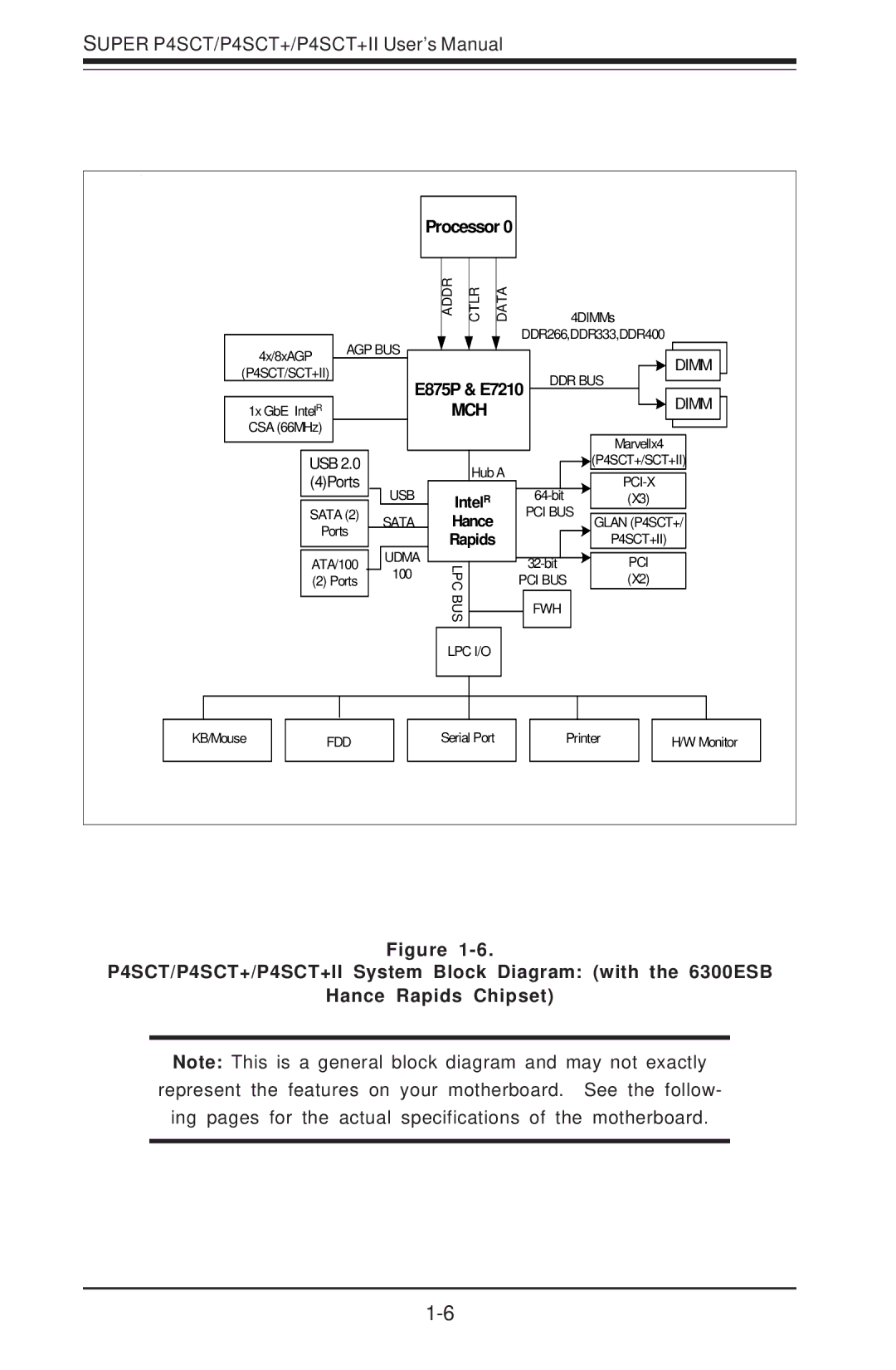
SUPER MICRO Computer has established a prominent reputation in the realm of high-performance computing solutions, and its line of motherboards, including the P4SCT+II, P4SCT, and P4SCT+, stands as a testament to their commitment to quality and innovation. These motherboards are designed primarily for Intel Pentium 4 processors, embodying the P4 chipset architecture that enhances reliability and performance in computing tasks.One of the significant features of the P4SCT+II is its support for dual-channel DDR SDRAM. This allows for increased memory bandwidth, which is crucial for demanding applications requiring rapid data processing. With a maximum memory capacity of 4GB, users can expect consistent performance even under heavy workloads. Moreover, these motherboards come equipped with a variety of PCI slots, including PCI Express, allowing for the addition of high-speed graphics cards, RAID controllers, and other expansion options that cater to specific user needs.
The P4SCT+II distinguishes itself with integrated features like the 10/100 Ethernet controller, which ensures seamless connectivity for networking applications. Additionally, the inclusion of several SATA ports facilitates fast data transfer rates for storage solutions, significantly boosting overall system performance. The motherboards also support IDE drives, ensuring versatility for users who prefer traditional storage solutions.
Power efficiency is another hallmark of SUPER MICRO's designs. The P4SCT+II, P4SCT, and P4SCT+ utilize an advanced power management system, optimizing power consumption without compromising performance. This approach not only enhances the longevity of the components but also contributes to eco-friendly computing practices.
From a thermal management perspective, these motherboards are engineered with robust cooling solutions. They provide ample fan headers and locations for passive heatsinks to maintain optimal operating temperatures. This feature is crucial for users who push their systems to the limit, whether for gaming, multitasking, or running resource-intensive applications.
In summary, the SUPER MICRO Computer P4SCT+II, P4SCT, and P4SCT+ motherboards exemplify a blend of advanced technology and practicality. With support for dual-channel DDR SDRAM, versatile PCI slots, integrated networking capabilities, and efficient power management, they cater to both professional and personal computing environments. These motherboards are ideal for anyone seeking high reliability and performance in their computing endeavors, making them a valuable investment in the world of technology.

