DEM-DAI3010 specifications
The Texas Instruments DEM-DAI3010 is a highly versatile evaluation module designed to showcase the capabilities of the AIC3101 family of audio codecs. This module is particularly suited for engineers looking to explore audio processing applications in various consumer electronics, telecommunications, and automotive industries. The DEM-DAI3010 serves as a powerful platform for testing and integrating audio technologies into prototypes and final products.One of the standout features of the DEM-DAI3010 is its high-performance audio processing capabilities. Equipped with a 24-bit audio data path and sampling rates of up to 192 kHz, the module ensures clear and high-fidelity sound reproduction. This feature makes the DEM-DAI3010 ideal for applications where sound quality is paramount, such as music playback systems, hearing aids, and professional audio equipment.
The DEM-DAI3010 utilizes Texas Instruments' advanced audio processing technologies, including programmable gain amplifiers, low-noise power supplies, and state-of-the-art digital signal processing (DSP). These technologies enable users to manipulate audio signals effectively, allowing for functions like audio mixing, equalization, and effects processing. Additionally, the module supports various audio formats, enhancing its adaptability to different project requirements.
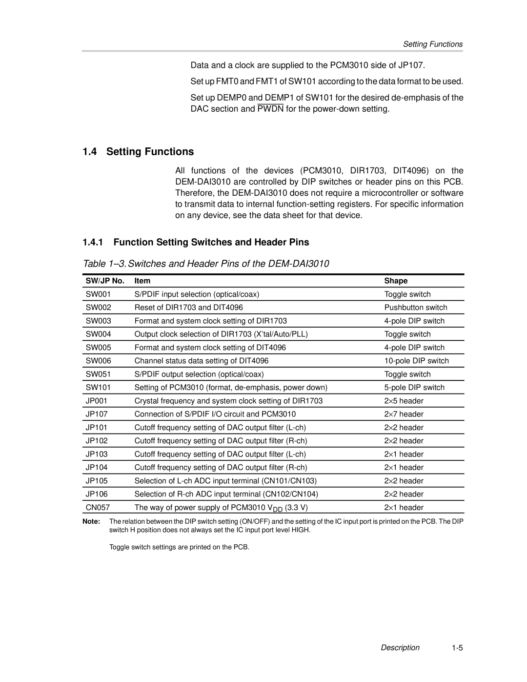
Another characteristic of the DEM-DAI3010 is its user-friendly interface, which includes an I^2C control interface for seamless communication and configuration. This flexibility facilitates rapid prototyping and system integration, allowing engineers to test their designs quickly and efficiently. The integrated 3.5mm audio jacks provide easy connectivity for audio inputs and outputs, making it simpler to interact with the module during development phases.
Also noteworthy is its compatibility with even lower-powered microcontrollers, which makes it more suitable for portable applications. This ensures that projects can maintain high audio performance without compromising on power efficiency.
Overall, the Texas Instruments DEM-DAI3010 stands out as an essential tool for engineers and developers in the audio technology space. Its combination of high-quality audio processing, flexible interfaces, and compatibility with a range of devices positions it as a valuable resource for exploring and implementing advanced audio solutions. Whether for prototyping or as part of a finished product, the DEM-DAI3010 offers a robust platform to harness the power of modern audio technologies.

