PGA309EVM-USB specifications
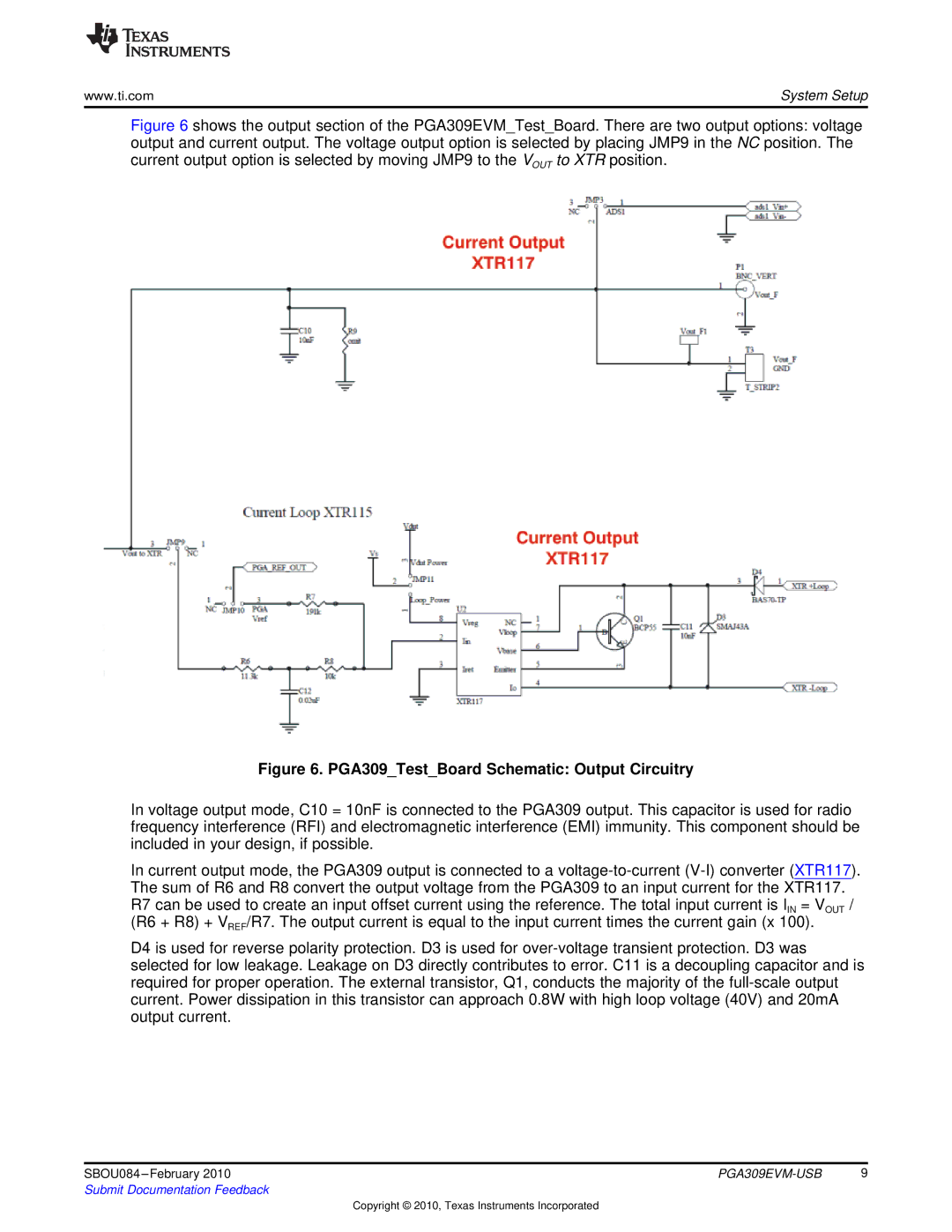
The Texas Instruments PGA309EVM-USB is an Evaluation Module designed specifically for the PGA309 Precision Analog Front End (AFE) family. This versatile and powerful device serves various applications in the realm of sensor signal conditioning, particularly for pressure sensors, temperature sensors, and other analog sensors requiring high precision.One of the main features of the PGA309EVM-USB is its high-performance PGA309 device, which incorporates a programmable gain amplifier (PGA) allowing for flexible signal amplification. The PGA309 has a gain range from 1 to 128, enabling it to adapt to a wide array of sensor types and output levels. This flexibility is crucial for achieving optimal performance in diverse applications.
The module also leverages advanced analog and digital processing technologies, which enhance its capabilities. It integrates an onboard microcontroller, allowing users to easily configure settings, execute control algorithms, and manage data acquisition. The built-in USB interface simplifies the communication with a PC, making it straightforward to control the EVM through intuitive software provided by Texas Instruments.
Another significant characteristic of the PGA309EVM-USB is its highly accurate signal conditioning features, such as offset and gain calibration, which ensure minimized errors and improved measurement reliability. The device supports a variety of digital output configurations, including I2C and SPI, to allow easy integration into different system architectures.
In addition to its robust signal processing core, the PGA309EVM-USB is designed with user-friendly interfaces, making it suitable for both experienced engineers and those new to sensor design. The comprehensive software toolkit offers a graphical user interface (GUI) that enables real-time monitoring and adjustment of parameters, ensuring users can optimize their applications.
Furthermore, the device is designed for functionality in harsh environments, incorporating features to withstand temperature variations and electrical noise. This reliability adds value for applications in industrial automation, automotive systems, and medical devices.
In summary, the Texas Instruments PGA309EVM-USB stands out as a powerful tool for engineers looking to design and prototype high-precision sensor signal conditioning applications. With its programmable gain amplifier, advanced processing capabilities, and user-friendly interfaces, it represents a significant advancement in the field of analog signal processing, allowing for greater flexibility and accuracy in diverse applications.

