Plug-N-Play Platform Inputs and Outputs

3.4 Control and Indicator Circuits

Three main control circuits are provided with the TPA032D03. The mute circuit grounds the output of the active amplifier, the mode circuit selects between the class-D amplifier and the headphone amplifier, and the shutdown circuit places the entire device into a power-saving sleep mode to minimize current consumption. Each of these inputs is TTL compatible: less than 0.8 V applied to these pins is considered a logic low, and any voltage greater than 2 V is considered a logic high.

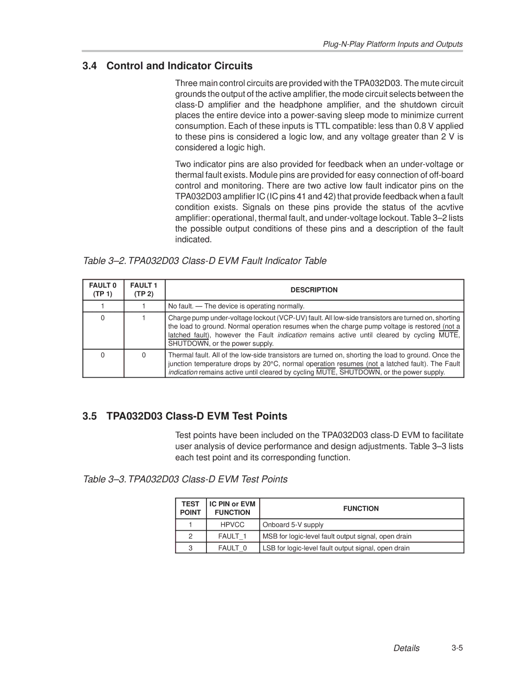
Two indicator pins are also provided for feedback when an under-voltage or thermal fault exists. Module pins are provided for easy connection of off-board control and monitoring. There are two active low fault indicator pins on the TPA032D03 amplifier IC (IC pins 41 and 42) that provide feedback when a fault condition exists. Signals on these pins provide the status of the acvtive amplifier: operational, thermal fault, and under-voltage lockout. Table 3±2 lists the possible output conditions of these pins and a description of the fault indicated.

Table 3±2. TPA032D03 Class-D EVM Fault Indicator Table

FAULT 0

FAULT 1

DESCRIPTION

(TP 1)

(TP 2)


1

1

No fault. Ð The device is operating normally.


0

1

Charge pump under-voltage lockout (VCP-UV) fault. All low-side transistors are turned on, shorting


the load to ground. Normal operation resumes when the charge pump voltage is restored (not a


latched fault), however the Fault indication remains active until cleared by cycling

MUTE,


SHUTDOWN, or the power supply.


0

0

Thermal fault. All of the low-side transistors are turned on, shorting the load to ground. Once the


junction temperature drops by 20°C, normal operation resumes (not a latched fault). The Fault


indication remains active until cleared by cycling MUTE, SHUTDOWN, or the power supply.


3.5 TPA032D03 Class-D EVM Test Points

Test points have been included on the TPA032D03 class-D EVM to facilitate user analysis of device performance and design adjustments. Table 3±3 lists each test point and its corresponding function.

Table 3±3. TPA032D03 Class-D EVM Test Points

TEST

IC PIN or EVM

FUNCTION

POINT

FUNCTION


1

HPVCC

Onboard 5-V supply


2

FAULT_1

MSB for logic-level fault output signal, open drain


3

FAULT_0

LSB for logic-level fault output signal, open drain

Details 3-5

Page 19
Image 19
Texas Instruments SLOU082 manual Control and Indicator Circuits, TPA032D03 Class-D EVM Test Points

SLOU082 specifications

Texas Instruments SLOU082 is a technical document primarily focused on the TPS7A47 device, which is an enhanced, low-noise linear voltage regulator designed for world-class performance in sensitive analog applications. This document explains the features, technologies, and characteristics that set the TPS7A47 apart in the industry.

One of the main features of the TPS7A47 is its ultra-low output noise, boasting a remarkable specification of just 1.2 μVRMS across a bandwidth of 10 Hz to 100 kHz. This characteristic makes it an ideal choice for high-precision, low-noise applications such as RF and audio signal processing, where minimizing noise is crucial for system performance. Additionally, the device offers a wide output voltage range from 1.4 V to 20 V, providing flexibility in various applications.

The TPS7A47 operates with a maximum output current of 1 A, enabling it to support multiple loads efficiently. Its dropout voltage is impressively low, particularly at light load conditions, ensuring high-efficiency performance in battery-powered applications. This aspect significantly extends battery life, making it suitable for portable devices.

Another highlight is the PowerPAD package offered for the TPS7A47, which enhances thermal performance and simplifies PCB design. The integration of thermal protection ensures the regulator operates safely under various conditions, preventing potential damage due to overheating.

The TPS7A47 also includes features such as reverse current protection, which prevents current from flowing back into the input when the output voltage exceeds the input voltage. This feature enhances reliability and extends the longevity of the device in various circuit configurations.

In terms of control, the TPS7A47 utilizes a low-dropout architecture, ensuring steady voltage regulation with minimal input-to-output voltage differential. It also supports a wide range of capacitor types, which allows for flexibility in component selection in layout design.

Overall, the Texas Instruments SLOU082 document on the TPS7A47 provides detailed insights into one of the most effective voltage regulation solutions available today. With exceptional noise performance, a versatile voltage range, robust thermal management, and reliability characteristics, the TPS7A47 is an exemplary choice for engineers and designers aiming to achieve high-performance analog systems.