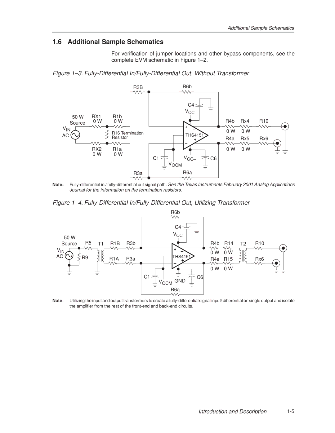
THS4151 specifications
Texas Instruments THS4151 is a high-performance analog amplifier designed to meet the needs of various applications where precision and low power consumption are critical. This device is known for its wide bandwidth, low noise, and high slew rate, making it suitable for high-speed signal processing in telecommunications, industrial automation, and medical devices.One of the main features of the THS4151 is its high bandwidth, with a gain bandwidth product of up to 50 MHz. This characteristic allows the amplifier to handle fast-changing signals efficiently, which is essential in modern electronic devices that require rapid response times. Furthermore, the THS4151 boasts a high slew rate of 100 V/µs, enabling it to accommodate fast signal swings without distortion, thus ensuring signal integrity across a variety of applications.
The THS4151 utilizes advanced complementary bipolar technology to achieve excellent performance while maintaining low power consumption. With a supply voltage range from 4.5 V to 12 V, the device can operate effectively in battery-operated systems, contributing to longer battery life and reduced power costs. The low quiescent current of only 5 mA further enhances its efficiency, making the THS4151 an ideal choice for portable electronics.
In addition to its impressive performance metrics, the THS4151 is designed with thermal stability in mind. Its built-in features help minimize drift and improve accuracy over a wide temperature range, which is particularly important for precision measurement applications. The device also offers a low input offset voltage and low input bias current, ensuring minimal errors in amplification.
Another key characteristic of the THS4151 is its compatibility with a wide range of input and output loads, making it versatile for different circuit configurations. The amplifier can be easily integrated into various designs, from simple feedback configurations to more complex signal conditioning applications.
Overall, the Texas Instruments THS4151 stands out as a leading choice in the high-speed amplifier market, combining advanced technology, low power consumption, and robust performance to meet the demands of today's sophisticated electronic designs. Whether used in audio processing, video signal enhancement, or sensor interfacing, the THS4151 delivers reliability and precision that engineers and designers can count on.

