Manuals
/
Transcend Information
/
Photography
/
Camera Accessories
Transcend Information
CF 266X
dimensions
TS2G~8GCF266
Models:
CF 266X
1
10
79
79
Download
79 pages
34.97 Kb
7
8
9
10
11
12
13
14
Specs
Block Diagram
Signal Description
„ Error Posting
Dimension
Card Configuration
„ Execute Drive Diagnostic 90h
CF-ATA Command Set
¾ Multiple Sector Setting
„ Check Power Mode 98h or E5h
Page 10
Image 10
TS2G~8GCF266
266X CompactFlash Card
Transcend Information Inc.
10
Page 9
Page 11
Page 10
Image 10
Page 9
Page 11
Contents
266X CompactFlash Card
Placement Features
Dimensions
Description
Transcend
Block Diagram
Pin Assignments and Pin Type
TS2G~8GCF266
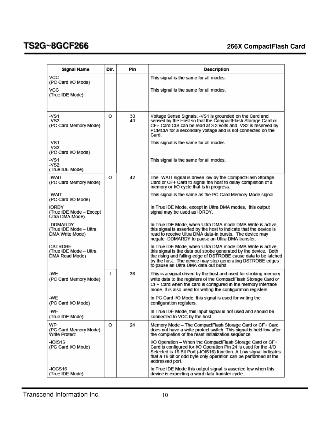
Signal Description
TS2G~8GCF266
TS2G~8GCF266
TS2G~8GCF266
TS2G~8GCF266
Electrical Specification
„ Output Drive Type „ Output Drive Characteristics
„ Signal Interface
„ Additional Requirements for CF Advanced Timing Modes
¾ Series termination required for Ultra DMA operation
266X CompactFlash Card
„ Ultra DMA Electrical Requirements
Table Typical Series Termination for Ultra DMA
¾ Ultra DMA Mode Cabling Requirement
„ Attribute Memory Read Timing Specification
TS2G~8GCF266
„ Common Memory Read Timing Specification
„ Common Memory Write Timing Specification
„ I/O Input Read Timing Specification
TS2G~8GCF266
„ I/O Output Write Timing Specification
TS2G~8GCF266
„ True IDE PIO Mode Read/Write Timing Specification
TS2G~8GCF266
„ True IDE Ultra DMA Mode Read/Write Timing Specification
Table Ultra DMA Data Burst Timing
266X CompactFlash Card
TS2G~8GCF266
TS2G~8GCF266
TS2G~8GCF266
„ Single Function CF+ Cards
Card Configuration
„ Multiple Function CF+ Cards
TS2G~8GCF266
„ Attribute Memory Function
Attribute Memory Function
TS2G~8GCF266
TS2G~8GCF266
„ Pin Replacement Register Base + 04h in Attribute Memory
„ Socket and Copy Register Base + 06h in Attribute Memory
Table Pcmcia Mode I/O Function
Transfer Function
Common Memory Transfer Function
Table Common Memory Function
True IDE Mode I/O Transfer Function
Metaformat Overview
CF-ATA Drive Register Set Definition and Protocol
„ I/O Primary and Secondary Address Configurations
Table Primary and Secondary I/O Decoding
„ Contiguous I/O Mapped Addressing
Table Contiguous I/O Decoding
„ True IDE Mode Addressing
„ Memory Mapped Addressing
„ CF-ATA Registers
¾ Data Register Address 1F0h170hOffset 0,8,9
¾ Cylinder High LBA 23-16 Register Address 1F5h175h Offset
¾ Sector Count Register Address 1F2h172h Offset
¾ Sector Number LBA 7-0 Register Address 1F3h173h Offset
¾ Drive/Head LBA 27-24 Register Address 1F6h176h Offset
TS2G~8GCF266
¾ Device Control Register Address 3F6h376h Offset Eh
¾ Card Drive Address Register Address 3F7h377h Offset Fh
CF-ATA Command Set
„ Check Power Mode 98h or E5h
„ Execute Drive Diagnostic 90h
„ Erase Sectors C0h
„ Flush Cache E7h
„ Format Track 50h
„ Identify Device Ech
266X CompactFlash Card
¾ Word 0 General Configuration
¾ Word 6 Default Number of Sectors per Track
¾ Word 1 Default Number of Cylinders
¾ Word 3 Default Number of Heads
¾ Word 49 Capabilities Bit 13 Standby Timer
¾ Translation Parameters Valid
¾ Multiple Sector Setting
¾ Total Sectors Addressable in LBA Mode
¾ Current Number of Cylinders, Heads, Sectors/Track
¾ Recommended Multiword DMA transfer cycle time
¾ Words 82-84 Features/command sets supported
¾ Word 65 Minimum Multiword DMA transfer cycle time
¾ Word 68 Minimum PIO transfer cycle time with Iordy
¾ Words 85-87 Features/command sets enabled
¾ Word 88 Ultra DMA Modes Supported and Selected
¾ Word 89 Time required for Security erase unit completion
¾ Word 128 Security Status Bit 8 Security Level
¾ Word 91 Advanced power management level value
¾ Word 160 Power Requirement Description
Additional Requirements for CF Advanced Timing Modes
TS2G~8GCF266
„ Idle 97h or E3h
„ Initialize Drive Parameters 91h
„ Idle Immediate 95h or E1h
„ NOP 00h
„ Read Buffer E4h
„ Read DMA C8h „ Read Long Sector 22h or 23h
TS2G~8GCF266
„ Recalibrate 1Xh „ Request Sense 03h
„ Seek 7Xh „ Set Features EFh
Feature Supported
266X CompactFlash Card
„ Standby Immediate 94h or E0h „ Translate Sector 87h
Translate Sector Information
„ Wear Level F5h „ Write Buffer E8h „ Write DMA CAh
TS2G~8GCF266
TS2G~8GCF266
„ Error Posting
TS2G~8GCF266
Top
Page
Image
Contents