Manuals
/
Transcend Information
/
Photography
/
Camera Accessories
Transcend Information
CF 266X
dimensions
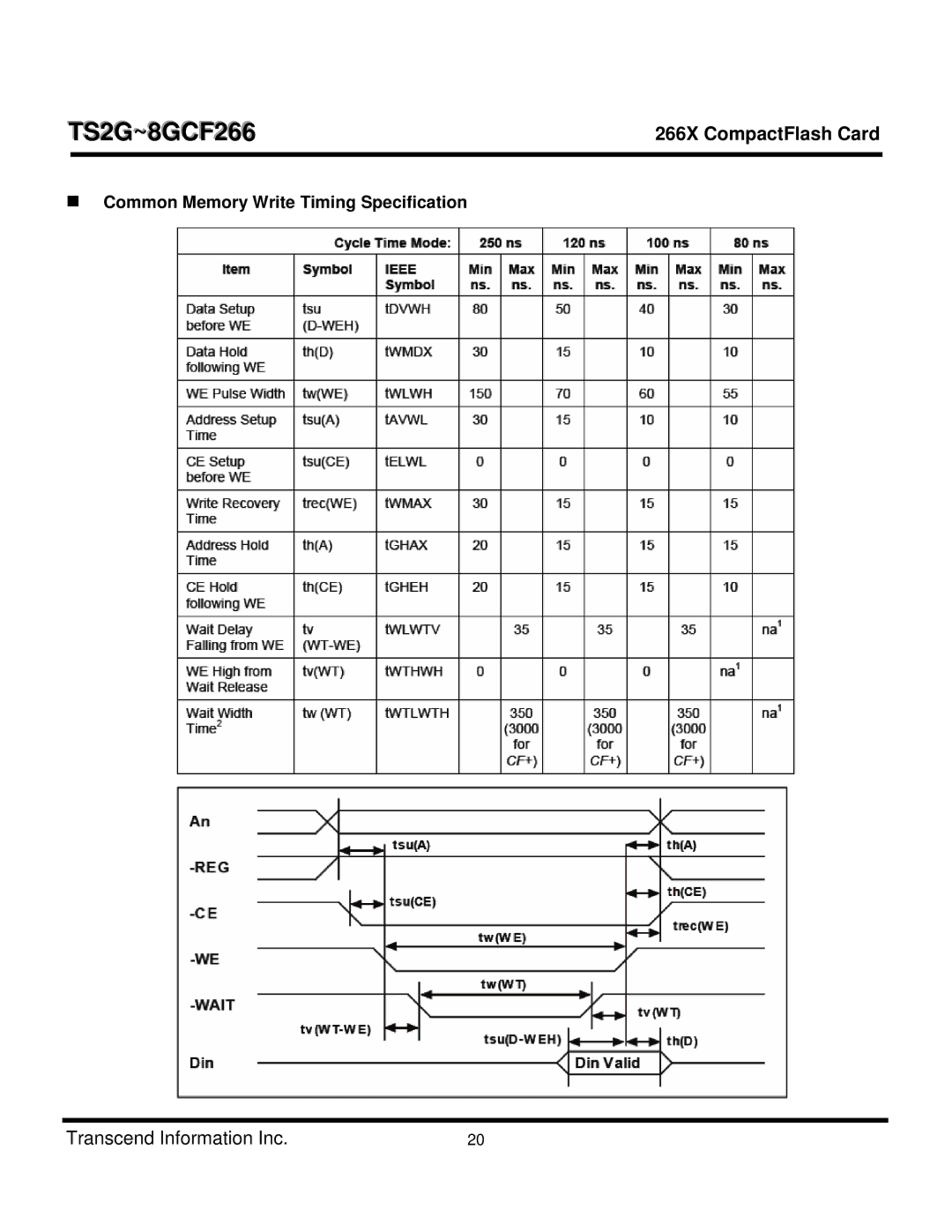
Common Memory Write Timing Specification
Models:
CF 266X
1
20
79
79
Download
79 pages
34.97 Kb
17
18
19
20
21
22
23
24
Specifications
Block Diagram
Signal Description
„ Error Posting
Dimension
Card Configuration
„ Execute Drive Diagnostic 90h
CF-ATA Command Set
¾ Multiple Sector Setting
„ Check Power Mode 98h or E5h
Page 20
Image 20
TS2G~8GCF266
266X CompactFlash Card
Common Memory Write Timing Specification
Transcend Information Inc.
20
Page 19
Page 21
Page 20
Image 20
Page 19
Page 21
Contents
Placement Features
Dimensions
266X CompactFlash Card
Description
Transcend
Block Diagram
Pin Assignments and Pin Type
TS2G~8GCF266
Signal Description
TS2G~8GCF266
TS2G~8GCF266
TS2G~8GCF266
TS2G~8GCF266
Electrical Specification
„ Output Drive Type „ Output Drive Characteristics
„ Signal Interface
„ Additional Requirements for CF Advanced Timing Modes
266X CompactFlash Card
„ Ultra DMA Electrical Requirements
¾ Series termination required for Ultra DMA operation
Table Typical Series Termination for Ultra DMA
¾ Ultra DMA Mode Cabling Requirement
„ Attribute Memory Read Timing Specification
TS2G~8GCF266
„ Common Memory Read Timing Specification
„ Common Memory Write Timing Specification
„ I/O Input Read Timing Specification
TS2G~8GCF266
„ I/O Output Write Timing Specification
TS2G~8GCF266
„ True IDE PIO Mode Read/Write Timing Specification
TS2G~8GCF266
„ True IDE Ultra DMA Mode Read/Write Timing Specification
Table Ultra DMA Data Burst Timing
266X CompactFlash Card
TS2G~8GCF266
TS2G~8GCF266
TS2G~8GCF266
„ Multiple Function CF+ Cards
Card Configuration
„ Single Function CF+ Cards
TS2G~8GCF266
„ Attribute Memory Function
Attribute Memory Function
TS2G~8GCF266
TS2G~8GCF266
„ Pin Replacement Register Base + 04h in Attribute Memory
„ Socket and Copy Register Base + 06h in Attribute Memory
Table Pcmcia Mode I/O Function
Transfer Function
Common Memory Transfer Function
Table Common Memory Function
True IDE Mode I/O Transfer Function
Metaformat Overview
CF-ATA Drive Register Set Definition and Protocol
„ I/O Primary and Secondary Address Configurations
Table Primary and Secondary I/O Decoding
„ Contiguous I/O Mapped Addressing
Table Contiguous I/O Decoding
„ True IDE Mode Addressing
„ Memory Mapped Addressing
„ CF-ATA Registers
¾ Data Register Address 1F0h170hOffset 0,8,9
¾ Sector Count Register Address 1F2h172h Offset
¾ Sector Number LBA 7-0 Register Address 1F3h173h Offset
¾ Cylinder High LBA 23-16 Register Address 1F5h175h Offset
¾ Drive/Head LBA 27-24 Register Address 1F6h176h Offset
TS2G~8GCF266
¾ Device Control Register Address 3F6h376h Offset Eh
¾ Card Drive Address Register Address 3F7h377h Offset Fh
CF-ATA Command Set
„ Check Power Mode 98h or E5h
„ Execute Drive Diagnostic 90h
„ Erase Sectors C0h
„ Flush Cache E7h
„ Format Track 50h
„ Identify Device Ech
266X CompactFlash Card
¾ Word 0 General Configuration
¾ Word 1 Default Number of Cylinders
¾ Word 3 Default Number of Heads
¾ Word 6 Default Number of Sectors per Track
¾ Word 49 Capabilities Bit 13 Standby Timer
¾ Multiple Sector Setting
¾ Total Sectors Addressable in LBA Mode
¾ Translation Parameters Valid
¾ Current Number of Cylinders, Heads, Sectors/Track
¾ Words 82-84 Features/command sets supported
¾ Word 65 Minimum Multiword DMA transfer cycle time
¾ Recommended Multiword DMA transfer cycle time
¾ Word 68 Minimum PIO transfer cycle time with Iordy
¾ Words 85-87 Features/command sets enabled
¾ Word 88 Ultra DMA Modes Supported and Selected
¾ Word 89 Time required for Security erase unit completion
¾ Word 91 Advanced power management level value
¾ Word 160 Power Requirement Description
¾ Word 128 Security Status Bit 8 Security Level
Additional Requirements for CF Advanced Timing Modes
TS2G~8GCF266
„ Idle 97h or E3h
„ NOP 00h
„ Idle Immediate 95h or E1h
„ Initialize Drive Parameters 91h
„ Read Buffer E4h
„ Read DMA C8h „ Read Long Sector 22h or 23h
TS2G~8GCF266
„ Recalibrate 1Xh „ Request Sense 03h
„ Seek 7Xh „ Set Features EFh
Feature Supported
266X CompactFlash Card
„ Standby Immediate 94h or E0h „ Translate Sector 87h
Translate Sector Information
„ Wear Level F5h „ Write Buffer E8h „ Write DMA CAh
TS2G~8GCF266
TS2G~8GCF266
„ Error Posting
TS2G~8GCF266
Top
Page
Image
Contents