User’s Manual
PCI-6872
Copyright
Optional item
Packing List
Additional Information and Assistance
FCC
PCI-6872 User’s Manual
Contents
Chapter Software Configuration
Appendix a Programming the Watchdog Timer
Appendix D System Assignments 109
112
Xii
General Information
Introduction
Features
Specifications
Standard SBC Functions
Solid State disk
2 VGA/LCD Interface
PCI bus Ethernet interface
Mechanical and Environmental
Board layout dimensioncomponent side
Board layout dimensions
Board layout dimension solder side
Installation
Connectors
Jumpers
Jumpers
CN9
Connectors
Jumper & Connector location
Locating Connectors&Jumperscomponent side
Connectors soldor side
Locating Connectorssolder side
Setting Jumpers
Cmos clear J1
Clear Cmos J1
Watchdog timer output option J2
Watchdog timer configuration
Watchdog timer output option J2
COM2 RS232-422-485 Select J3
ATX power control connector CN20,CN21
Installing DIMMs
Printer port connector CN4
CompactFlash Card connector
CompactFlash CN5
IDE connectorCN1,CN2
Floppy drive connector CN3
Connecting the floppy drive
Connecting the hard drive
Flat panel display connector CN22
CRT display connector CN7
Extension flat panel connectorCN23
Lvds LCD panel connector CN25
USB connectors CN6
Panel type selectionSW1
S1 Panel Type Select SW1
Ethernet configuration
Power connectors CN14, CN15
ATX Power & HDD LED, speaker out Connector CN16, CN17, CN19
Keyboard and PS/2 mouse connector CN11
COM port connectorCN9,CN10, CN29
External KB/mouse connector CN12
Watchdog output CN18
Daughter card connector CN27,CN28
Software Configuration
Mode
VGA display firmware configuration
VGA setup screen
PCI-6872 User’s Manual
Award Bios Setup
System test and initialization
System configuration verification
Entering setup
Award Bios setup
Cmos Features setup
Standard Cmos Features setup
Advanced Bios Features setup
Advanced Bios Features setup
Advanced Chipset Features setup
Advanced Chipset Features setup
Integrated Peripherals
Power Management Setup
PC Health Status
7 PnP/PCI Configurations
Frequency/Voltage Control
Frequency/Voltage Control
Set Password
Load Optimized Defaults
11 Establish Password
Exit Without Saving
Save & Exit Setup
PCI Svga Setup
Chipset
Display memory
Display types
Installation for Windows
Installation of the Svga Driver
PCI-6872 User’s Manual
\Biscuit\9577\VGA\Win9xMe
PCI-6872 User’s Manual
Installation for Windows 98/Me
Select Adapter, then Change
PCI Svga Setup
Insert the CD into the CD-ROM drive. Type in the path
PCI Svga Setup
Installation for Windows NT
Choose the Settings tab, and press the Display Type button
Press the Change... button
\Biscuit\VGA\WinNT
PCI-6872 User’s Manual
Press OK to reboot
Installation for Windows
Choose the Video Controller VGA Compatible button
Choose the Drive button, press Update Driver... button
PCI Svga Setup
PCI-6872 User’s Manual
Installation for Windows XP
Choose Hardware and Device Manager, press OK button
Choose Video Controller VGA Compatible, press OK but- ton
PCI-6872 User’s Manual
PCI Svga Setup
PCI-6872 User’s Manual
Further Information
PCI-6872 User’s Manual
PCI Bus Ethernet Inter- face
Installation of Ethernet driver
Installation for MS-DOS and Windows
PCI Bus Ethernet Interface
PCI Bus Ethernet Interface
PCI-6872 User’s Manual
PCI Bus Ethernet Interface
Installation for Windows
Choose the Driver tab press Update Driver...button
Choose Display a list
PCI Bus Ethernet Interface
PCI-6872 User’s Manual
Installation for Windows NT
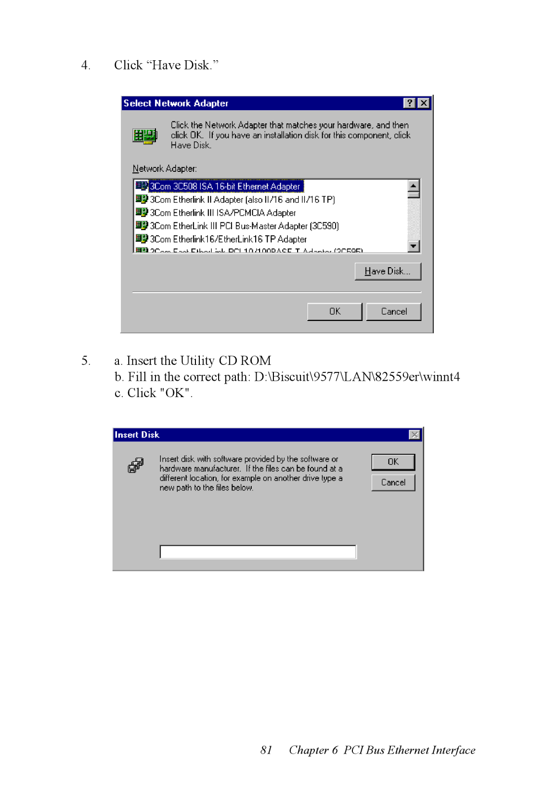
Choose type of network. b. Click Next Click Select from list
PCI Bus Ethernet Interface
Check the highlighted item, and click OK
PCI Bus Ethernet Interface
PCI-6872 User’s Manual
Realtek website Intel website Advantech websites
PCI-6872 User’s Manual
Programming the Watchdog Timer
Supported Input Timing Modes
Appendix a Programming the Watchdog Timer
Return
PCI-6872 User’s Manual
Pin Assignments
ATX power feature connectorCN20
Table B.1 ATX power feature connector CN20
Appendix B Pin Assignments
Floppy Disk Drive Disk connector CN3
Parallel Port ConnectorCN4
Table B.2 Parallel Port connector CN4
Table B.3 Floppy Disk Drive Connector CN3
Table B.4 IDE HDD connector CN1,CN2
IDE Hard Drive Connector CN1,CN2
Table B.5 CompactFlash Card ConnectorCN5
ConpactFlash card connector CN5
Table B.6 CRT Display Connector CN7
CRT Display Connector CN7
LAN, RJ45 Connector CN8
USB Connector CN6
Table B.7 USB Connector CN6
Table B.8 LAN, RJ45 Connector CN8
Table B.9 Main Power ConnectorCN15
Main Power Connector CN15
Table B.10 ATX Power LED and KB-Lock ConnectorCN16
ATX power LED and KB-Lock connector CN16
Speaker Out CN17
Table B.11 Speaker OutCN17
Table B.12 Watchdog Output ConnectorCN18
Watchdog output connector CN18
HDD LED CN19
Table B.13 HDD LEDCN19
Table B.14 Power ButtonCN21
PowerButton CN21
Table B.15 Flat Panel ConnectorCN22
Flat Panel Connector CN22
Table B.16 Extension Flat Panel ConnectorCN23
Extension flat panel connector CN23
COM Connector CN9, CN10, CN29
Lvds LCD connector CN25
Table B.17 Lvds LCD ConnectorCN25
Table B.18 COM connector CN9, CN10, CN29
LCD Inverter Backlight Connector CN24
19 COM2 Extension connector RS422-RS485CN29
Table B.19 COM2 Extension Connector RS422-RS485CN29
Table B.20 LCD Inverter Backlight ConnectorCN24
CPU Fan Power connectorCN14
Keyboard and PS/2Mouse Connector CN11
Table B.21 Keyboard and mouse connector CN11
Table B.22 FAN connector CN14
24 I/O daughter board connector1CN27
Table B.23 External KB/Mouse ConnectorCN12
Table B.24 I/O Daughter Board Connector1CN27
Table B.25 I/O Daughter Board Connector1CN28
25 I/O daughter board connector1 CN28
System Assignments
Appendix D System Assignments
System I/O Ports
Table D.1 System I/O ports
DMA channel assignments
1st MB memory map
Table D.2 1st MB memory map
Table D.3 DMA channel assignments
Table D.4 Interrupt assignments
Interrupt assignments