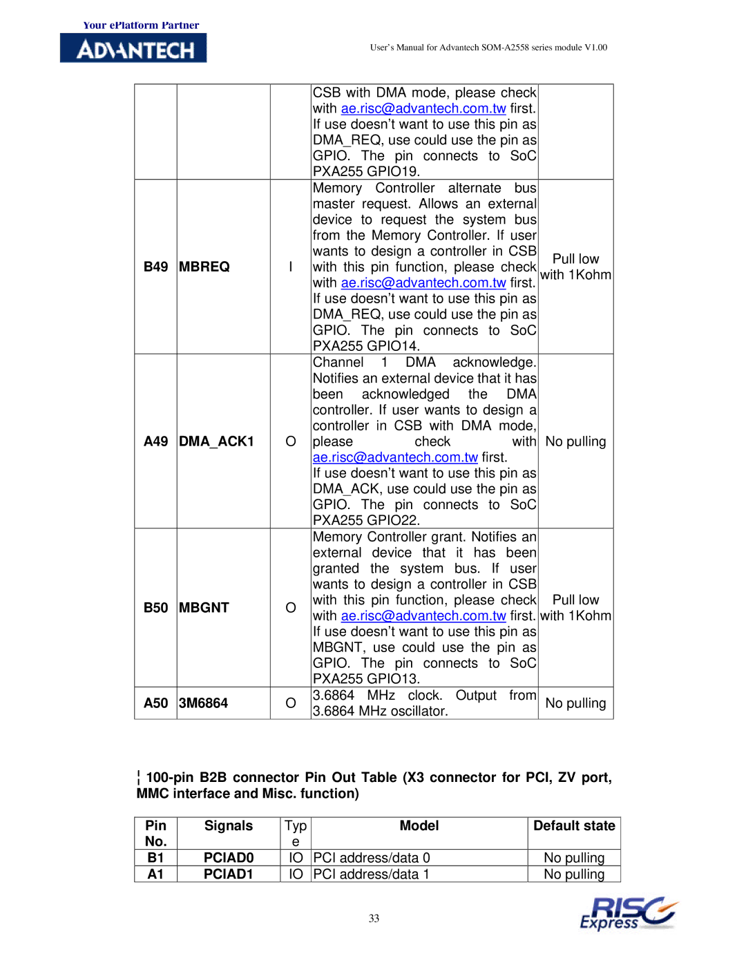
SOM-A2558 specifications
The Advantech SOM-A2558 represents a significant advancement in system-on-module (SOM) technology, designed to meet the needs of demanding applications in industries such as industrial automation, transportation, and smart cities. Featuring the Intel Apollo Lake processor, specifically the dual-core or quad-core options, the SOM-A2558 delivers an optimal blend of performance and efficiency.At the core of the SOM-A2558 is the Intel Atom E3950 or E3940 processors, which enable robust processing capabilities while maintaining low power consumption. This is crucial for embedded systems that require continuous operation in energy-sensitive environments. The module supports up to 8GB of DDR4 memory, enhancing its multitasking abilities and enabling it to handle complex applications with ease.
One of the standout features of the SOM-A2558 is its extensive array of I/O options, including USB 3.0, UART, I2C, SPI, and GPIO. This versatility allows for seamless integration with various peripherals and sensors, making it ideal for IoT applications and industrial automation systems. The SOM also supports dual Gigabit Ethernet ports, providing high-speed network connectivity essential for real-time data transfer and communications.
In terms of graphics, the SOM-A2558 supports Intel HD Graphics, which enhances the visual performance for display applications. With integrated hardware-accelerated video decoding and support for 4K resolution, it is suitable for applications such as digital signage and multimedia processing.
Advantech has designed the SOM-A2558 for durability and reliability, featuring a wide operating temperature range from -40°C to 85°C, making it suitable for harsh environments. Additionally, the module's compact form factor ensures easy integration into various system designs, allowing developers to create tailored solutions without significant space constraints.
The SOM-A2558 also supports multiple storage options, including eMMC, SATA III, and M.2 interfaces, which provide flexibility for different storage needs and configurations. Its support for TPM 2.0 enhances security, a vital aspect for applications handling sensitive data.
In summary, the Advantech SOM-A2558 combines cutting-edge technology, extensive connectivity options, and robust performance to facilitate the development of innovative solutions across various sectors. Its features make it an excellent choice for developers looking to create reliable and efficient embedded systems.

