Appendix A – Configuration Straps
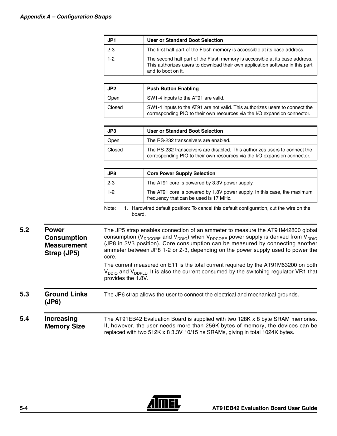
JP1 | User or Standard Boot Selection |
|
|
The first half part of the Flash memory is accessible at its base address. | |
|
|
The second half part of the Flash memory is accessible at its base address. | |
| This authorizes users to download their own application software in this part |
| and to boot on it. |
|
|
JP2 | Push Button Enabling |
|
|
Open | |
|
|
Closed | |
| corresponding PIO to their own resources via the I/O expansion connector. |
|
|
JP3 | User or Standard Boot Selection |
|
|
Open | The |
|
|
Closed | The |
| corresponding PIO to their own resources via the I/O expansion connector. |
|
|
JP8 | Core Power Supply Selection |
|
|
The AT91 core is powered by 3.3V power supply. | |
|
|
The AT91 core is powered by 1.8V power supply. In this case, the maximum | |
| frequency that can be used is 17 MHz. |
|
|
|
| Note: 1. Hardwired default position: To cancel this default configuration, cut the wire on the |
|
| board. |
|
|
|
5.2 | Power | The JP5 strap enables connection of an ammeter to measure the AT91M42800 global |
| Consumption | consumption (VDDCORE and VDDIO) when VDDCORE power supply is derived from VDDIO |
| Measurement | (JP8 in 3V3 position). Core consumption can be measured by connecting another |
| Strap (JP5) | ammeter between JP8 |
| core. | |
|
|
The current measured on E11 is the total current required by the AT91M63200 on both
VDDIO and VDDPLL. It is also the current consumed by the switching regulator VR1 that provides the 1.8V.
5.3Ground Links The JP6 strap allows the user to connect the electrical and mechanical grounds.
(JP6)
5.4Increasing Memory Size
The AT91EB42 Evaluation Board is supplied with two 128K x 8 byte SRAM memories. If, however, the user needs more than 256K bytes of memory, the devices can be replaced with two 512K x 8 3.3V 10/15 ns SRAMs, giving in total 1024K bytes.
AT91EB42 Evaluation Board User Guide
