PB6200, PB6100 specifications
The BenQ PB6100 is a versatile and user-friendly projector designed for both home and office use. As an entry-level projector, it provides impressive specifications, making it ideal for presentations, movie watching, and educational purposes.One of the standout features of the BenQ PB6100 is its brightness. With a luminous output of up to 3,200 ANSI lumens, it can perform well even in well-lit environments. This ensures that images remain vibrant and clear, regardless of the ambient lighting conditions. Paired with a 2000:1 contrast ratio, the PB6100 delivers sharp and detailed images, allowing for enhanced color accuracy and depth.
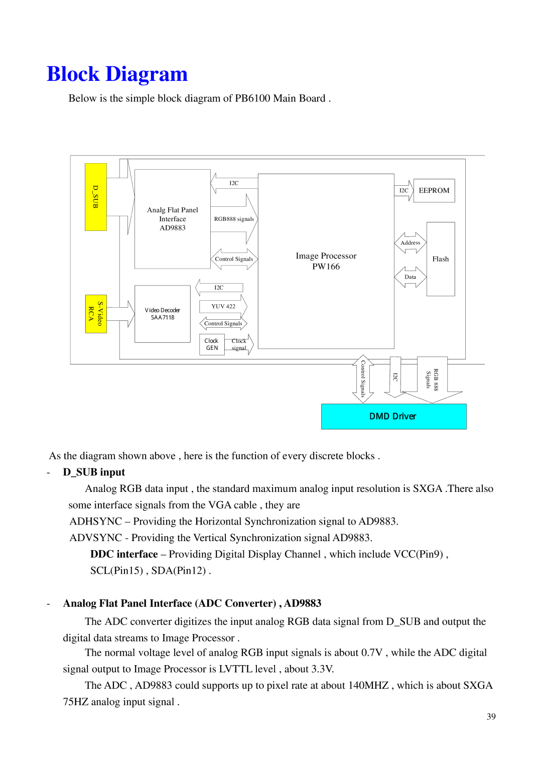
The PB6100 employs DLP (Digital Light Processing) technology, which is known for its reliability and image quality. This technology utilizes a digital micromirror device that creates images with remarkable clarity and precision. The DLP design also ensures fewer maintenance issues, as it is less susceptible to dust accumulation compared to other projector types.
Another notable characteristic of the BenQ PB6100 is its resolution capability. It supports a native SVGA resolution of 800 x 600 pixels, which is suitable for basic presentations and video playback. It also supports various aspect ratios, including 4:3 and 16:9, providing flexibility depending on the content being presented.
In addition to its performance features, the PB6100 offers several connectivity options. It is equipped with multiple input ports, including VGA, USB, and composite video, allowing users to connect various devices such as laptops, desktops, and DVD players. This wide range of connections enhances the projector’s versatility in different setups.
Portability is another attribute of the BenQ PB6100. Designed to be lightweight and compact, it is easy to transport for off-site meetings or home entertainment.
The projector also has built-in speakers, which provide decent sound output, eliminating the need for additional audio equipment in casual viewing settings.
In summary, the BenQ PB6100 blends functionality with user-centric designs, making it an exceptional choice for those seeking an affordable projector without compromising on quality. Its features, such as high brightness, DLP technology, variety of connectivity options, and portable design, position it as a solid option for any user looking to enhance their visual experience.

