Initial reset
When batteries are set or an AC adapter is connected, the reset IC provides a low pulse to the CPU. The CPU then initializes its internal circuit and clears data in the working strage RAM.
Power ON reset
When the power switch is pressed, the CPU receives a low pulse of POWER signal. The CPU first raises APO signal to +5V to generat DVDD voltage, then raises RESET signal to +5V. During this period the gate array, the DSP and the key touch LSI initializes their internal circuit.
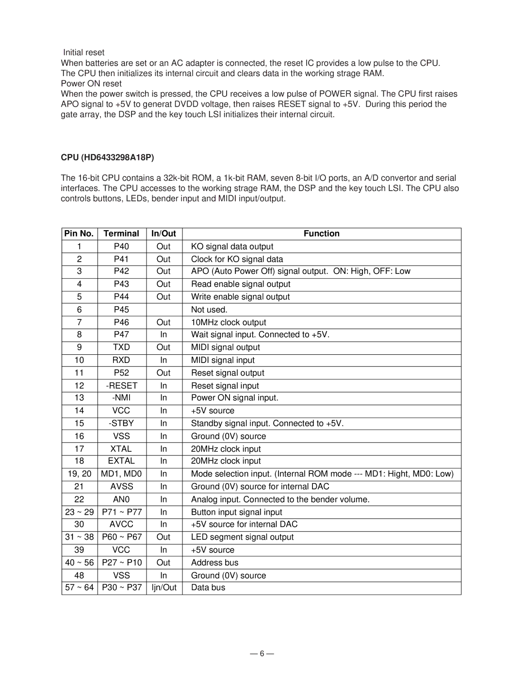
CPU (HD6433298A18P)
The
Pin No. | Terminal | In/Out | Function |
|
|
|
|
1 | P40 | Out | KO signal data output |
|
|
|
|
2 | P41 | Out | Clock for KO signal data |
|
|
|
|
3 | P42 | Out | APO (Auto Power Off) signal output. ON: High, OFF: Low |
|
|
|
|
4 | P43 | Out | Read enable signal output |
|
|
|
|
5 | P44 | Out | Write enable signal output |
|
|
|
|
6 | P45 |
| Not used. |
|
|
|
|
7 | P46 | Out | 10MHz clock output |
|
|
|
|
8 | P47 | In | Wait signal input. Connected to +5V. |
|
|
|
|
9 | TXD | Out | MIDI signal output |
|
|
|
|
10 | RXD | In | MIDI signal input |
|
|
|
|
11 | P52 | Out | Reset signal output |
|
|
|
|
12 | In | Reset signal input | |
|
|
|
|
13 | In | Power ON signal input. | |
|
|
|
|
14 | VCC | In | +5V source |
|
|
|
|
15 | In | Standby signal input. Connected to +5V. | |
|
|
|
|
16 | VSS | In | Ground (0V) source |
|
|
|
|
17 | XTAL | In | 20MHz clock input |
|
|
|
|
18 | EXTAL | In | 20MHz clock input |
|
|
|
|
19, 20 | MD1, MD0 | In | Mode selection input. (Internal ROM mode |
|
|
|
|
21 | AVSS | In | Ground (0V) source for internal DAC |
|
|
|
|
22 | AN0 | In | Analog input. Connected to the bender volume. |
|
|
|
|
23 ~ 29 | P71 ~ P77 | In | Button input signal input |
|
|
|
|
30 | AVCC | In | +5V source for internal DAC |
|
|
|
|
31 ~ 38 | P60 ~ P67 | Out | LED segment signal output |
|
|
|
|
39 | VCC | In | +5V source |
|
|
|
|
40 ~ 56 | P27 ~ P10 | Out | Address bus |
|
|
|
|
48 | VSS | In | Ground (0V) source |
|
|
|
|
57 ~ 64 | P30 ~ P37 | Ijn/Out | Data bus |
|
|
|
|
— 6 —
