Page
Page
D900C/D901C
Trademarks
About this Manual
Important Safety Instructions
Instructions for Care and Operation
Power Safety
Battery Precautions
Preface
Contents
DVI/ CRT
Introduction
Feature Specification
System Specifications
System Specifications 1
Option
Physical
Top View
External Locator Top View with LCD Panel Open
Front Views
External Locator Front & Rear Views
Left Side View
External Locator Left & Right Side View
Right Side View
Bottom View
External Locator Bottom View
Mainboard Top Key Parts
Mainboard Overview Top Key Parts
Mainboard Bottom Key Parts
Mainboard Overview Bottom Key Parts
Mainboard Top Connectors
Mainboard Overview Top Connectors
Mainboard Bottom Connectors
Mainboard Overview Bottom Connectors
Introduction
Overview
Disassembly
Disassembly
Maintenance Precautions
Disassembly
Disassembly Steps
Battery Removal
Removing the Battery
Optical Device Removal
Removing the Optical CD/DVD Device
Removing the Hard Disk Drive
HDD Assembly Removal
Removing the Hard Disks in the Secondary HDD Bay
Assembly Removal
RAM Module Removal
Removing the System Memory RAM
Contact Warning
RAM Module Removal cont’d
Processor Removal
Removing the Processor
VGA Card Removal
Removing the VGA Card
VGA Card Removal Cont’d
VGA Card Installation
Installing the VGA Card
Keyboard Removal
Removing the Keyboard
Wireless LAN Module Removal
Removing the Wireless LAN Module
Bluetooth Module Removal
Removing the Bluetooth Module
Modem Removal
Removing the Modem
TV Tuner Card Removal
Removing the TV Tuner Card
Disassembly
Appendix APart Lists
Part List Illustration Location
Part List Illustration Location
TOP D900C D901C
TOP D900C/D901C
Bottom D900C
Bottom D900C/D901C
LCD D900C/D901C
MB One VGA only D900C/D901C
MB One VGA only D900C/D901C
MB D900C/D901C
MB D900C/D901C
HDD D900C D901C
HDD D900C/D901C
2nd HDD D900C D901C
2nd HDD D900C/D901C
Combo D900C
Combo D900C/D901C
DVD-DUAL RW D900C/D901C
DVD-DUAL RW D900C/D901C
Part Lists
Schematic Diagrams
Appendix BSchematic Diagrams
Block Diagram
Block Diagram
Sheet 1
Sheet 2
Clock Generator
Clock Generator
Vcore
CPU-1
Sheet 3
CPU-1
Sheet 4
CPU-2
CPU-2
Sheet 5 Intel P965 CPU Interace
Intel P965 CPU Interface 1/4
PE0RX0 PE0TXC0
MCHBSEL0
MCHBSEL1
MCHBSEL2
Sheet 7 Intel P965 Memory I/F
Intel P965 Memory I/F 3/4
3VS
Ddrii Sodimm
Sheet 8
Ddrii Sodimm
Sheet 9 Intel P965 Power
Intel P965 Power 4/4
Sheet 10 of 40 ICH8 PCI, DMI
ICH8 PCI, DMI, CPU, IRQ
CPU, IRQ
Sheet 11 of 40 ICH8 LPC, ATA
ICH8 LPC, ATA, USB, Gpio
USB, Gpio
Sheet 12 ICH8 Power
ICH8 Power
2VS 9,15..17,30
Sheet 13
MXM PCI-E CON1
MXM PCI-E CON1
Sheet 14
MXM PCI-E CON2
MXM PCI-E CON2
Sheet 15 BR03 PCI-E & Strap
BR03 PCI-E & Straps 1/3
Interface 2/3
BR03 PCI-E Interface 2/3
Sheet 16
BR03 PCI-E
BR03 Power & GND
BR03 Power & GND 3/3
Sheet 18
DVI/ CRT
DVI/ CRT
Sheet 19 Panel Con LED Indicator
Panel CON/ LED Indicator
10,28 AD0..31
1394/ Card Reader TI PCI7402
CARDPWREN#
Sheet 21
Glan RTL8111B
Glan RTL8111B
Sheet 22 Audio ALC888 Amplifier
Audio ALC888/ Amplifier
Sheet 23 of 40 KBC-H8/2111
KBC-H8/2111
Pata
JM368 Pcie to Pata
Mini Card & TV Out/ Video
Sheet 26 Daughter Connection
Daughter Connection
Sheet 27 of 40 CCD/ BT/ FAN
CCD/ BT/ FAN/ ROM
ROM
Sheet 28 Mini PCI/ MDC New Card
Mini PCI/ MDC/ New Card
Sheet 29 of 40 AC-In, Charger
AC-In, Charger
25VS 6,9,12 2VS 2VS 4..6,9,12,15..17
Power 1.2V
Sheet 30 Power 1.2V
VDD5 19,23,26,31,33
13,14 RUNPWROK#
Power 1.5V/ 1.05V
Sheet 31 Power 1.5V
19,23,26,30,33 VDD5
Vtten
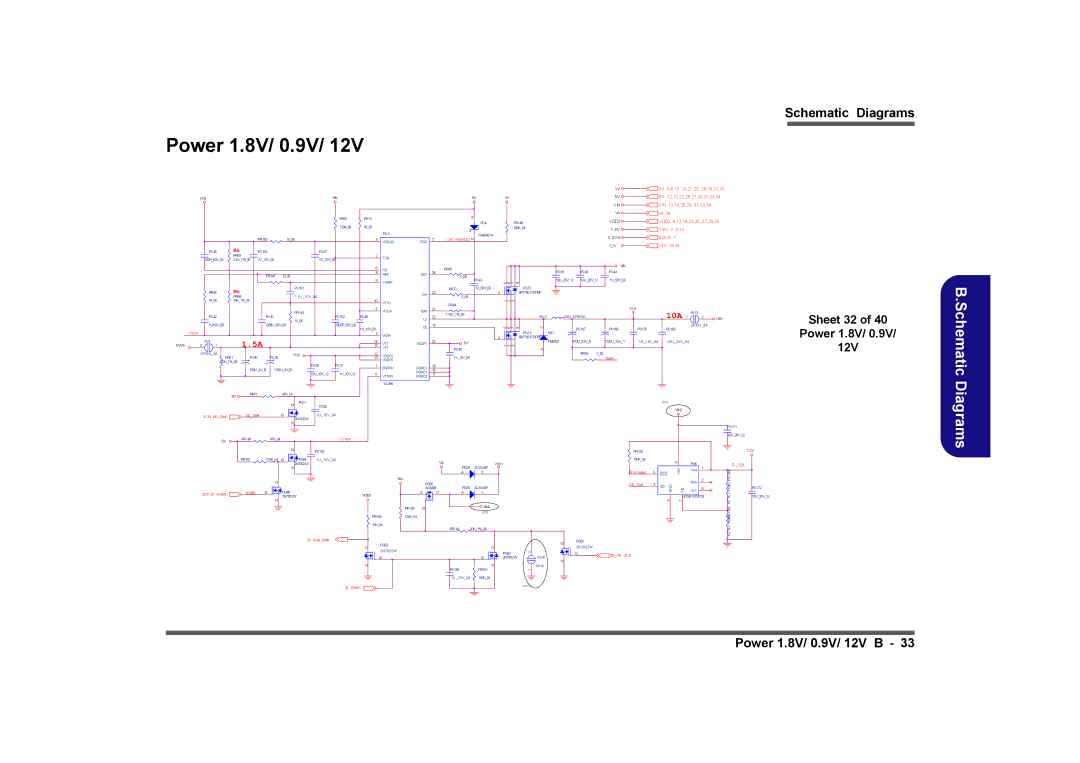
Sheet 32 Power 1.8V 12V
8VPWRGD C
Vssa
VIN 13,19,26,29..32,34
VDD5 19,23,26,30,31 10..13,21,25..28,30..32
5VS 4,9..13,25,28
5VS 6,12..14,18,19,22,24,26..28
Vttpwgd
VCore Power
VIN
Vcoreon
Sheet 35 Audio Board
Audio Board
Sheet 36 Card Reader Board
Card Reader Board
SWR
Click Board
Sheet 37 Click Board
Tpaddatac Tpadclkc
Sheet 38 HotKey Board
HotKey Board
Sheet 39 of 40 Switch Board
Switch Board
PRG GND
USBN4F USBP4F USBN6F USBP6F
USB Board
Sheet 40 USB Board
USBP0F SBN0F SBP2F SBN2F
Schematic Diagrams