Manuals
/
Clevo
/
Computer Equipment
/
Laptop
Clevo
manual
Combo Drive M570A/M575A
Models:
M575A
1
48
94
94
Download
94 pages
53.07 Kb
45
46
47
48
49
50
51
52
Specification
Appendix BSchematic Diagrams
Bluetooth
Wireless LAN Module Removal
Maintenance
Mainboard Top Connectors
Disassembly
Battery Precautions
Weight
Safety
Page 48
Image 48
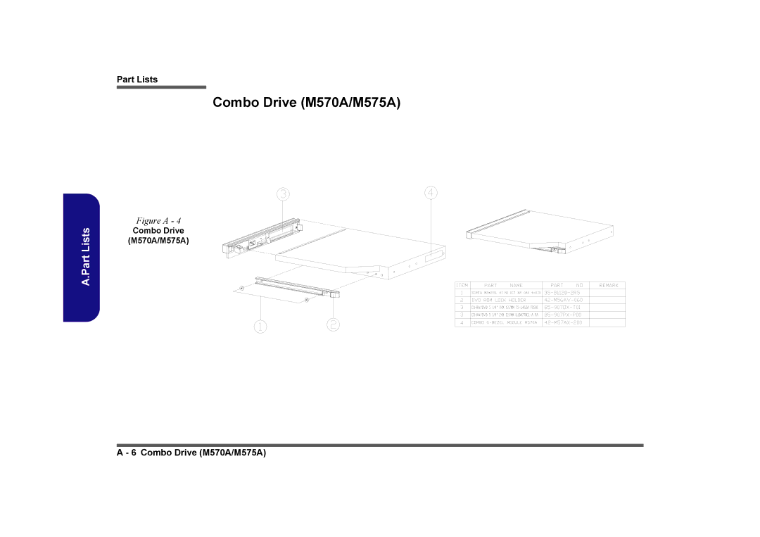
A.Part Lists
Part Lists
Combo Drive (M570A/M575A)
Figure A - 4
Combo Drive
(M570A/M575A)
A - 6 Combo Drive (M570A/M575A)
Page 47
Page 49
Page 48
Image 48
Page 47
Page 49
Contents
Page
Page
M570A/M575A
Trademarks
About this Manual
Important Safety Instructions
Instructions for Care and Operation
Power Safety
Battery Precautions
Related Documents
Contents
AUDIO-DJ
Introduction
System Specifications
Feature Specification
System Specifications 1
Pcmcia
Weight Optional
Model difference
External Locator Top View with LCD Panel Open
Top View
External Locator Front Audio DJ& Rear Views
Front Views
Rear Views
External Locator Left Side & Right Side View
Left Side View
Right Side View
External Locator Bottom View
Bottom View
M570A/M575A Mainboard Overview Top Key Parts
Mainboard Top Key Parts
M570A/M575A Mainboard Overview Bottom Key Parts
Mainboard Bottom Key Parts
M570A/M575A Mainboard Overview Top Connectors
Mainboard Top Connectors
M570A/M575A Mainboard Overview Bottom Connectors
Mainboard Bottom Connectors
14 M570A/M575A Mainboard Overview Bottom Connectors
Disassembly
Overview
Disassembly
Maintenance Precautions
Disassembly Steps
Removing the Battery
Battery Removal
HDD Assembly Removal
Removing the Hard Disk Drive
Removing the System Memory RAM
RAM Module Removal
Removing the Wireless LAN Module
Wireless LAN Module Removal
Removing the Bluetooth Module
Bluetooth Module Removal
Removing the TV Tuner Card
TV Tuner Removal
Removing the Optical CD/DVD Device
Optical Device Removal
Removing the Processor
Processor Removal
Processor Removal Cont’d
Lock Unlock
Removing the VGA Card
VGA Card Removal
Removing the Keyboard
Keyboard Removal
Removing the Keyboard
Appendix APart Lists
Part List Illustration Location
Part List Illustration Location
Top M570A/M575A
Top M570A M575A
Bottom M570A/M575A
Bottom M570A M575A
LCD M570A/M575A
LCD M570A M575A
Combo Drive M570A/M575A
Combo Drive M570A/M575A
DVD Drive M570A/M575A
DVD Drive M570A/M575A
DVD-RW Drive M570A/M575A
DVD-RW Drive M570A/M575A
HDD M570A/M575A
HDD M570A M575A
Second-HDD M570A/M575A
Second HDD M570A/M575A
Appendix BSchematic Diagrams
Schematic Diagrams
System Block Diagram
Sheet 1 System Block Diagram
Clock Generator
Sheet 2
Clock Generator
CPU-1
CPU-2
Sheet 4
CPU-2
Alviso-1
Sheet 5 Alviso-1
Alviso-2
Sheet 6 Alviso-2
Alviso-3
Sheet 7 Alviso-3
Dimm a
Sheet 8
Dimm a
Dimm B
Sheet 9
Dimm B
VGA Card Connector
VGA Card Connector
Sheet 10
ICH6M-1
Sheet 11
ICH6M-1
ICH6M-2
Sheet 12
ICH6M-2
ICH6M-3
Sheet 13
ICH6M-3
VCC5REF
USB & CCD Conn
Sheet 14
USB & CCD Conn
Card BUS
Sheet 15 Card BUS
Card BUS &1394-2
Sheet 16 Card BUS
Sheet 17
Minipci
Realtek Giga LAN
Sheet 18
Realtek Giga LAN
Pcie Giga LAN
Sheet 19
Pcie Giga LAN
AC97
Sheet 20 AC97
AUDIO-DJ
Sheet 21
AUDIO-DJ
Azalia Codec & AMP
Sheet 22 Azalia Codec
AMP
Pre Amp AP8202
Sheet 23 Pre Amp AP8202
FRONT-L
Prerout
SIO FWH IR & CIR
Sheet 24
SIO FWH IR & CIR
Sheet 25
SRSCNTL# CCDDET# KB-SI4 H8CURSEN
Vcore
PMPSI# HVID5
SD#
+1.05VS, +2.5VS
Sheet 28 +1.8V, 0.9, +1.5V
SUSB#
Systemon
Mchpg
+VDD3, +VDD5, +VDD12
Sheet 29 of 40 +VDD3, +VDD5, +VDD12
CHARGER, DC
Sheet 30
CHARGER, DC
Button Board
Sheet 31
Card Reader Board
Sheet 32
Card Reader Board
USB Board M560A
Sheet 33
USB Board
M560A
USB Board M570A
Sheet 34
M570A
COM Port Board
Sheet 35
Audio DJ Board
Sheet 36
Audio DJ Board
Click Board
Sheet 37
Click Board
Pata HDD Board
Sheet 38
Pata HDD Board
Sata HDD Board
Sheet 39
Sata HDD Board
Second HDD Board
Sheet 40
Second HDD Board
Schematic Diagrams
Top
Page
Image
Contents