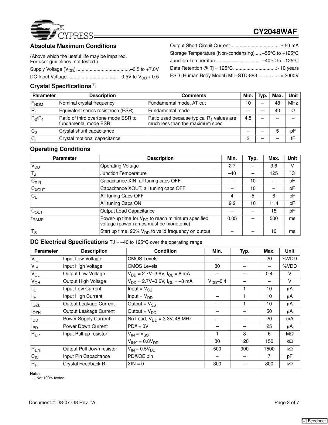
CY2048WAF specifications
The Cypress CY2048WAF is a highly integrated, low-power, real-time clock (RTC) chip designed for a variety of applications that require accurate timekeeping and minimal power consumption. One of the standout features of the CY2048WAF is its ability to maintain precise time in battery-operated devices while operating at extremely low energy levels. This makes it an ideal choice for portable electronics, wearables, and IoT devices where battery life is a critical consideration.At the heart of the CY2048WAF is its exceptional timekeeping accuracy, which is achieved through the use of a temperature-compensated crystal oscillator (TCXO). This oscillator ensures stability over a wide range of operating temperatures, resulting in long-term time accuracy and reliability. With an integrated power management system, the CY2048WAF can switch between different power modes, allowing it to conserve energy during periods of inactivity.
One of the key technologies integrated into the CY2048WAF is the I2C communication protocol, which simplifies the connection to microcontrollers and other digital systems. The ability to interface seamlessly with various devices makes the CY2048WAF a versatile choice for designers looking to incorporate precise timing functionality across different platforms.
The CY2048WAF also features a built-in alarm function, providing users with the ability to set alarms for various time intervals. This is particularly beneficial in applications where reminders or scheduled events are essential. Additionally, the device includes temperature sensors, enabling it to monitor ambient conditions and adapt its timekeeping functions accordingly.
Another noteworthy characteristic of the CY2048WAF is its compact package size, which allows for easier integration into space-constrained designs. With its low-profile form factor, the chip can be utilized in a variety of devices without significantly increasing the overall size or weight.
In conclusion, the Cypress CY2048WAF is an advanced RTC solution that combines accuracy, low power consumption, and a range of features that enhance its functionality in various applications. Its integration of cutting-edge technologies and thoughtful design make it an excellent choice for developers seeking reliable timekeeping solutions in portable and battery-operated devices.

