Cypress CY2309NZ manual Features, Functional Description, Logic Block Diagram

Models: CY2309NZ

1 6
Download 6 pages 14.54 Kb
Page 1
Image 1
CY2309NZ

CY2309NZ

Nine-Output 3.3V Buffer

Features

Functional Description

One-input to nine-output buffer/driver

Supports two DIMMs or four SO-DIMMs with one additional output for feedback to an external or chipset PLL

Low power consumption for mobile applications

Less than 32 mA at 66.6 MHz with unloaded outputs

1-ns Input-Output delay

Buffers all frequencies from DC to 133.33 MHz

Output-output skew less than 250 ps

Multiple VDD and VSS pins for noise and electromagnetic inter- ference (EMI) reduction

Space-saving 16-pin 150-mil SOIC package

3.3V operation

Industrial temperature available

The CY2309NZ is a low-cost buffer designed to distribute high-speed clocks in mobile PC systems and desktop PC systems with SDRAM support. The part has nine outputs, eight of which can be used to drive two DIMMs or four SO-DIMMs, and the remaining can be used for external feedback to a PLL. The device operates at 3.3V and outputs can run up to 133.33 MHz.

The CY2309NZ is designed for low EMI and power optimization. It has multiple VSS and VDD pins for noise optimization and consumes less than 32 mA at 66.6 MHz, making it ideal for the
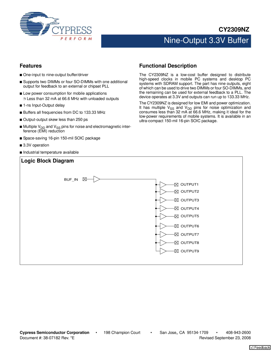
 low-power requirements of mobile systems. It is available in an ultra-compact 150-mil 16-pin SOIC package.

Logic Block Diagram

BUF_IN

OUTPUT1

OUTPUT2

OUTPUT3

OUTPUT4

OUTPUT5

OUTPUT6

OUTPUT7

OUTPUT8

OUTPUT9

Cypress Semiconductor Corporation • 198 Champion Court

San Jose, CA 95134-1709

408-943-2600

Document #: 38-07182 Rev. *E


Revised September 23, 2008

[+] Feedback

Page 1
Image 1
Cypress CY2309NZ manual Features, Functional Description, Logic Block Diagram, Nine-Output 3.3V Buffer