CY2309NZ
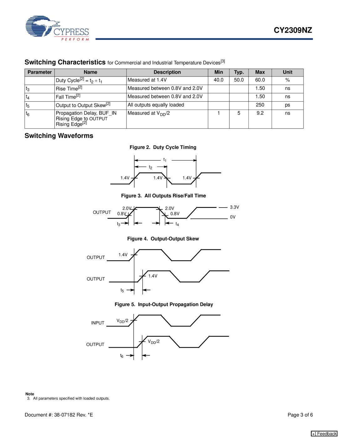
Switching Characteristics for Commercial and Industrial Temperature Devices[3]
Parameter | Name | Description | Min | Typ. | Max | Unit |
| Duty Cycle[2] = t2 ⎟ t1 | Measured at 1.4V | 40.0 | 50.0 | 60.0 | % |
t3 | Rise Time[2] | Measured between 0.8V and 2.0V |
|
| 1.50 | ns |
t4 | Fall Time[2] | Measured between 0.8V and 2.0V |
|
| 1.50 | ns |
t5 | Output to Output Skew[2] | All outputs equally loaded |
|
| 250 | ps |
t6 | Propagation Delay, BUF_IN | Measured at VDD/2 | 1 | 5 | 9.2 | ns |
| Rising Edge to OUTPUT |
|
|
|
|
|
| Rising Edge[2] |
|
|
|
|
|
Switching Waveforms
Figure 2. Duty Cycle Timing
|
| t1 |
| t2 |
|
1.4V | 1.4V | 1.4V |
Figure 3. All Outputs Rise/Fall Time
OUTPUT |
| 2.0V |
|
|
|
|
|
|
|
|
|
|
|
|
|
|
|
|
|
| 2.0V |
|
|
|
|
|
|
|
|
| 3.3V | |||||||||||||||||
|
|
|
|
|
|
|
|
|
|
|
|
|
|
|
|
|
|
| ||||||||||||||||||||||||||||||
|
|
|
|
|
|
|
|
|
|
|
|
|
|
|
|
|
|
|
|
|
| |||||||||||||||||||||||||||
|
|
|
|
|
|
|
|
|
|
|
|
|
|
|
|
|
|
|
|
|
|
|
|
|
| |||||||||||||||||||||||
0.8V |
|
|
|
|
|
|
|
|
|
|
|
|
|
|
|
|
|
|
|
|
|
| 0.8V |
|
|
|
|
| 0V | |||||||||||||||||||
|
|
|
|
|
|
|
|
|
|
|
|
|
|
|
|
|
|
|
|
| ||||||||||||||||||||||||||||
|
|
|
|
|
|
|
|
|
|
|
|
|
|
|
|
|
|
|
|
|
|
|
|
|
|
|
|
|
|
|
|
|
|
|
|
|
|
|
|
|
|
|
|
|
|
|
| |
|
|
|
| t3 |
|
|
|
|
|
|
|
|
|
|
|
|
|
|
|
|
|
|
|
|
|
|
|
|
|
|
| t4 |
|
|
|
|
|
| ||||||||||
|
|
|
|
|
|
|
|
|
|
|
|
|
|
|
|
|
|
|
|
|
|
|
|
|
|
|
|
|
|
|
|
|
|
|
|
| ||||||||||||
|
|
|
|
|
|
|
|
|
|
|
|
|
|
|
|
|
|
|
|
|
|
|
|
|
|
| ||||||||||||||||||||||
|
|
|
|
|
|
| Figure 4. |
|
|
|
|
|
| |||||||||||||||||||||||||||||||||||
OUTPUT |
| 1.4V |
|
|
|
|
|
|
|
|
|
|
|
|
|
|
|
|
|
|
|
|
|
|
|
|
|
|
|
|
|
|
|
|
|
|
| |||||||||||
|
|
|
|
|
|
|
|
|
|
|
|
|
|
|
|
|
|
|
|
|
|
|
|
|
|
|
|
|
|
|
|
|
|
| ||||||||||||||
|
|
|
|
|
|
|
|
|
|
|
|
|
|
|
|
|
|
|
|
|
|
|
|
|
|
|
|
|
|
|
|
|
|
| ||||||||||||||
|
|
|
|
|
|
|
|
|
|
|
|
|
|
|
|
|
|
|
|
|
|
|
|
|
|
|
|
|
|
|
|
|
|
|
|
|
|
|
|
|
|
|
|
| ||||
|
|
|
|
|
|
|
|
|
|
|
|
|
|
|
|
|
|
|
|
|
|
|
|
|
|
|
|
|
|
|
|
| ||||||||||||||||
OUTPUT |
|
|
|
|
|
|
|
|
|
|
|
|
|
|
|
|
| 1.4V |
|
|
|
|
|
| ||||||||||||||||||||||||
|
|
|
|
|
|
|
|
|
|
|
|
|
|
|
|
|
|
|
|
|
|
| ||||||||||||||||||||||||||
|
|
|
|
|
|
|
|
|
|
|
|
|
|
|
|
|
|
|
|
|
|
|
|
|
|
|
|
|
|
|
|
|
|
|
|
|
|
|
|
|
|
|
|
| ||||
|
|
|
| t5 |
|
|
|
|
|
|
|
|
|
|
|
|
|
|
|
|
|
|
|
|
|
|
|
|
|
|
|
|
|
|
|
|
|
|
| |||||||||
|
|
|
|
|
|
|
|
|
|
|
|
|
|
|
|
|
|
|
|
|
|
|
|
|
|
|
|
|
|
|
|
|
|
|
|
|
|
| ||||||||||
|
|
|
|
|
|
|
|
|
|
|
|
|
|
|
|
|
|
|
|
|
|
|
|
|
|
|
|
|
|
|
|
|
|
|
|
|
|
|
|
|
|
|
|
|
|
|
|
|
Figure 5. Input-Output Propagation Delay
INPUT | VDD/2 |
OUTPUT | VDD/2 |
| t6 |
Note
3. All parameters specified with loaded outputs.
Document #: | Page 3 of 6 |
[+] Feedback