CY62136VN MoBL®
2-Mbit (128K x 16) Static RAM
Features
•Temperature Ranges
—Industrial:
—
—
•High speed: 55 ns
•Wide voltage range:
•
•Easy memory expansion with CE and OE features
•
•Automatic
•CMOS for optimum speed/power
•Available in standard
Functional Description[1]
The CY62136VN is a
portable applications such as cellular telephones. The device also has an automatic
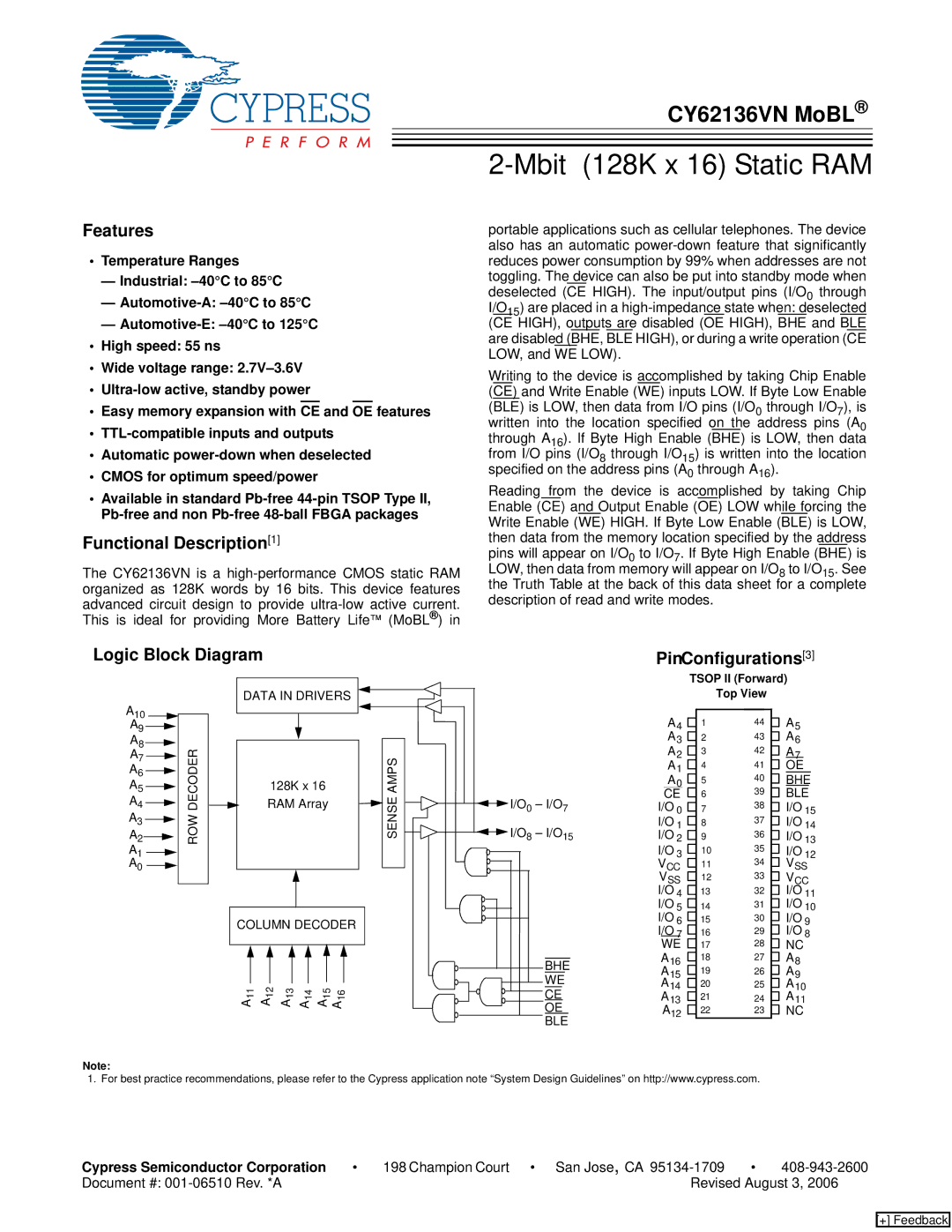
Writing to the device is accomplished by taking Chip Enable (CE) and Write Enable (WE) inputs LOW. If Byte Low Enable (BLE) is LOW, then data from I/O pins (I/O0 through I/O7), is written into the location specified on the address pins (A0 through A16). If Byte High Enable (BHE) is LOW, then data from I/O pins (I/O8 through I/O15) is written into the location specified on the address pins (A0 through A16).
Reading from the device is accomplished by taking Chip Enable (CE) and Output Enable (OE) LOW while forcing the Write Enable (WE) HIGH. If Byte Low Enable (BLE) is LOW, then data from the memory location specified by the address pins will appear on I/O0 to I/O7. If Byte High Enable (BHE) is LOW, then data from memory will appear on I/O8 to I/O15. See the Truth Table at the back of this data sheet for a complete description of read and write modes.
Logic Block Diagram
PinConfigurations[3]
A10
A9 ![]()
![]()
DATA IN DRIVERS ![]()
![]()
![]()
![]()
TSOP II (Forward)
Top View
A4 |
| 1 | 44 |
| A5 |
|
| ||||
|
|
A8 |
|
| DECODER | ||
|
| ||||
A7 |
| ||||
| |||||
A4 |
| ||||
A6 |
|
| |||
A5 |
|
| |||
A3 |
|
|
| ROW | |
|
|
| |||
A2 |
|
|
| ||
|
|
| |||
A1 |
|
| |||
|
| ||||
A0 |
|
| |||
|
| ||||
128K x 16 RAM Array
![]()
![]()
![]()
![]() SENSE AMPS
SENSE AMPS
![]()
![]()
![]()
![]() I/O0 – I/O7
I/O0 – I/O7
![]()
![]()
![]() I/O8 – I/O15
I/O8 – I/O15
| A3 |
| 43 |
|
| A6 |
|
| |||
| 2 |
|
|
| |||||||
|
|
|
| ||||||||
| A2 |
| 3 | 42 |
|
| A7 |
|
| ||
|
|
|
| ||||||||
|
|
|
| ||||||||
| A1 |
| 4 | 41 |
|
| OE |
|
| ||
|
|
|
| ||||||||
| A0 |
| 5 | 40 |
|
| BHE |
| |||
|
| ||||||||||
|
| ||||||||||
| CE |
|
| 6 | 39 |
|
| BLE | |||
I/O 0 |
| 38 |
|
| I/O 15 | ||||||
| 7 |
| |||||||||
|
|
| |||||||||
I/O | 1 |
|
| 37 |
|
| I/O 14 | ||||
|
| 8 |
| ||||||||
|
| ||||||||||
I/O | 2 |
|
| 36 |
|
| I/O 13 | ||||
|
| 9 |
| ||||||||
|
| ||||||||||
I/O 3 |
| 10 | 35 |
|
| I/O 12 | |||||
|
|
|
| ||||||||
VCC |
| 11 | 34 |
|
| VSS | |||||
|
| ||||||||||
VSS |
| 12 | 33 |
|
| VCC | |||||
|
| ||||||||||
I/O | 4 |
|
| 13 | 32 |
|
| I/O | 11 | ||
|
| ||||||||||
I/O | 5 |
|
| 14 | 31 |
|
| I/O | 10 | ||
|
| ||||||||||
I/O |
|
|
|
| 30 |
|
| I/O |
|
| |
COLUMN DECODER |
|
|
|
|
|
|
|
|
|
|
|
|
|
|
|
|
| |||||||||||
|
|
|
|
|
|
|
|
|
|
|
|
|
|
|
|
| ||||||||||||
|
|
|
|
|
|
|
|
|
|
|
|
|
|
|
|
|
|
|
|
|
|
|
|
|
|
|
|
|
|
|
|
|
|
|
|
|
|
|
|
|
|
|
|
|
|
|
|
|
|
|
|
|
|
|
|
|
|
|
|
|
|
|
|
|
|
|
|
|
|
|
|
|
|
|
|
|
|
|
|
|
|
|
|
| BHE | |
|
|
|
|
|
|
|
|
|
|
|
|
|
|
|
|
|
|
|
|
|
|
|
|
|
|
| ||
|
|
|
|
|
|
|
|
|
|
|
|
|
|
|
|
|
|
|
|
|
|
|
|
|
|
| WE | |
11 | 12 | 13 | 14 | 15 | 16 |
|
|
|
|
|
|
|
|
|
|
|
|
|
|
| CE | |||||||
A | A | A | A | A A |
|
|
|
|
|
|
|
|
|
|
|
|
|
|
| OE | ||||||||
|
|
|
|
|
|
|
|
|
|
|
|
|
|
|
|
| ||||||||||||
|
|
|
|
|
|
|
|
|
|
|
|
|
|
|
|
|
|
|
|
|
|
|
|
|
|
| ||
|
|
|
|
|
|
|
|
|
|
|
|
|
|
|
|
|
|
|
|
|
|
|
|
|
|
| BLE |
|
|
|
|
|
|
|
|
|
|
|
|
|
|
|
|
|
|
|
|
|
|
|
|
|
|
|
| ||
|
|
|
|
|
|
|
|
|
|
|
|
|
|
|
|
|
|
|
|
|
|
|
|
|
|
| ||
I/O 76 |
| 15 | 29 |
| I/O 89 |
|
| ||||
| 16 |
| |||
|
| ||||
WE |
| 17 | 28 |
| NC |
A16 |
| 18 | 27 |
| A8 |
|
| ||||
|
| ||||
A15 |
| 19 | 26 |
| A9 |
|
| ||||
A14 |
| 20 | 25 |
| A10 |
|
| ||||
A13 |
| 21 | 24 |
| A11 |
|
| ||||
A12 |
| 22 | 23 |
| NC |
|
|
Note:
1. For best practice recommendations, please refer to the Cypress application note “System Design Guidelines” on http://www.cypress.com.
Cypress Semiconductor Corporation | • | 198 Champion Court • San Jose, CA | • | |
Document #: |
| Revised August 3, 2006 | ||
[+] Feedback