CY62136VN MoBL®
Thermal Resistance[6]
Parameter | Description | Test Conditions | TSOPII | FBGA | Unit |
ΘJA | Thermal Resistance | Still Air, soldered on a 4.25 x 1.125 inch, | 60 | 55 | °C/W |
| (Junction to Ambient) |
|
|
| |
ΘJC | Thermal Resistance |
| 22 | 16 | °C/W |
| (Junction to Case) |
|
|
|
|
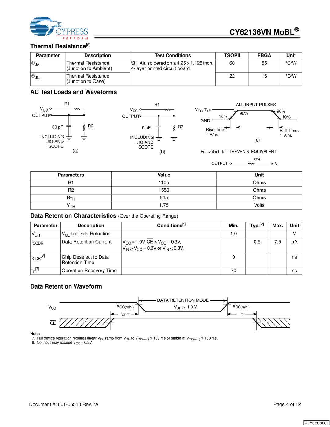
AC Test Loads and Waveforms
R1
VCC ![]()
OUTPUT![]()
30 pF
INCLUDING
JIG AND
SCOPE
(a)
R1
VCC ![]()
OUTPUT![]()
R2 | 5 pF |
|
INCLUDING
JIG AND
SCOPE
(b)
| VCC Typ |
|
|
|
|
|
|
|
| ALL INPUT PULSES |
|
|
| ||||
|
|
|
|
|
|
|
|
|
|
|
| 90% | |||||
| 10% |
|
|
|
|
|
| 90% |
|
|
|
|
| 10% | |||
|
|
|
|
|
|
|
|
|
|
|
|
|
| ||||
R2 | GND |
|
|
|
|
|
|
|
|
|
|
|
|
|
|
| |
|
|
|
|
|
|
|
|
|
|
|
|
|
|
| |||
Rise Time: |
|
|
|
|
|
|
|
|
|
|
| Fall Time: | |||||
|
|
|
|
|
|
|
|
|
|
|
| ||||||
| 1 V/ns |
|
|
|
|
|
|
|
|
|
|
| 1 V/ns | ||||
(c)
Equivalent to: THÉVENIN EQUIVALENT
RTH
OUTPUT ![]()
![]()
![]()
![]()
![]()
![]()
![]()
![]() V
V
Parameters | Value | Unit |
R1 | 1105 | Ohms |
|
|
|
R2 | 1550 | Ohms |
|
|
|
RTH | 645 | Ohms |
VTH | 1.75 | Volts |
Data Retention Characteristics (Over the Operating Range)
Parameter | Description |
|
| Conditions[9] | Min. | Typ.[2] | Max. | Unit |
VDR | VCC for Data Retention |
|
|
| 1.0 |
|
| V |
ICCDR | Data Retention Current | VCC = 1.0V, |
| > VCC − 0.3V, |
| 0.5 | 7.5 | ∝A |
CE |
| |||||||
|
| VIN > VCC − 0.3V or VIN < 0.3V, |
|
|
|
| ||
tCDR[6] | Chip Deselect to Data |
|
|
| 0 |
|
| ns |
| Retention Time |
|
|
|
|
|
|
|
t [7] | Operation Recovery Time |
|
|
| 70 |
|
| ns |
R |
|
|
|
|
|
|
|
|
Data Retention Waveform
 DATA RETENTION MODE
V | VCC(min.) | V | > 1.0 V | VCC(min.) |
CC |
| DR |
|
|
| tCDR |
|
| tR |
CE |
|
|
|
|
Note:
7.Full device operation requires linear VCC ramp from VDR to VCC(min) > 100 ms or stable at VCC(min) > 100 ms.
8.No input may exceed VCC + 0.3V
Document #: | Page 4 of 12 |
[+] Feedback