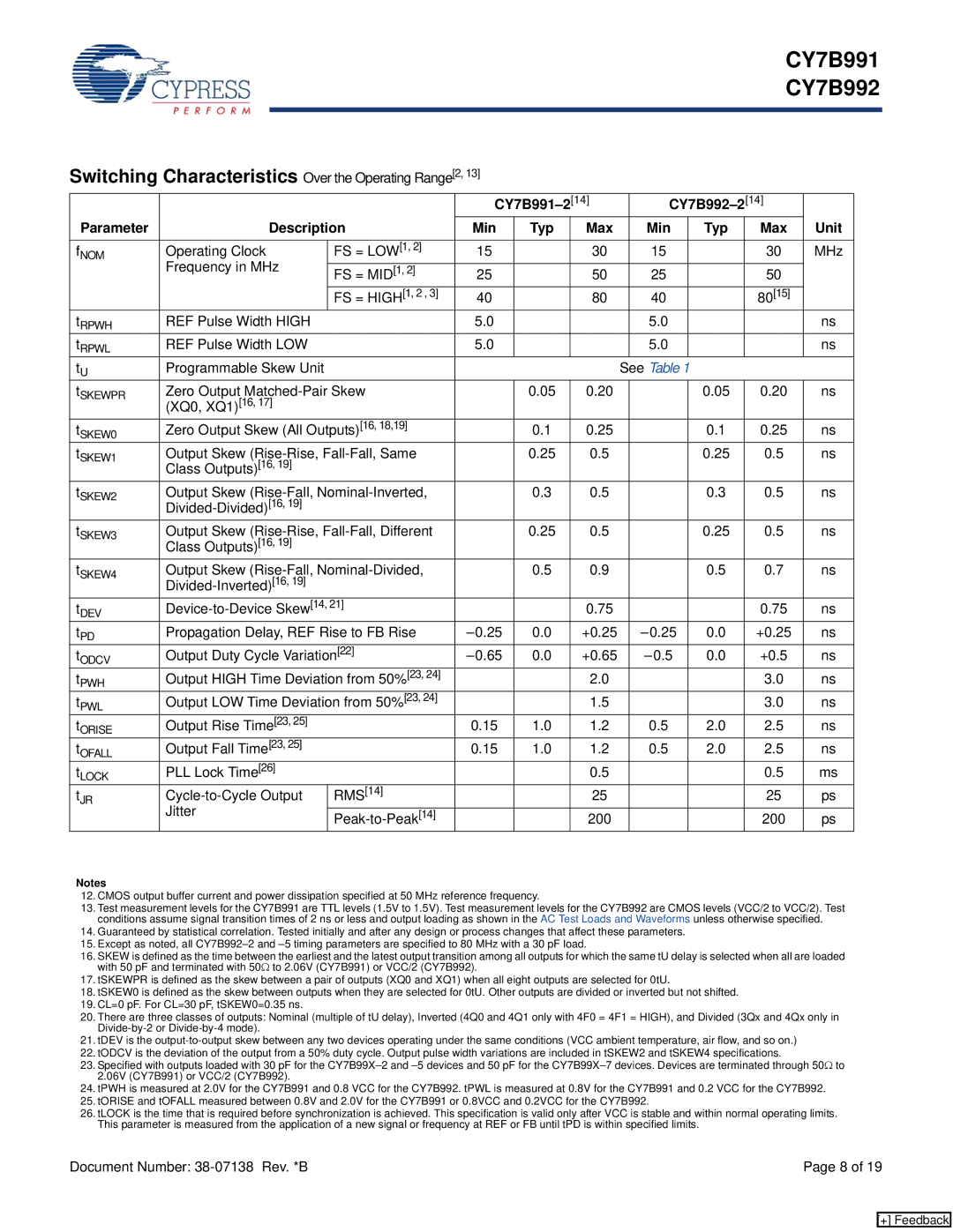
CY7B991, CY7B992 specifications
The Cypress CY7B992 and CY7B991 are advanced synchronous SRAM devices designed for high-speed applications, particularly in the field of telecommunications, networking, and high-performance computing. These SRAMs are notable for their ability to operate at high frequencies, making them suitable for systems that require rapid data access and processing.One of the main features of the CY7B992 and CY7B991 is their support for synchronous operation, which allows for data transfers aligned with a clock signal. This capability significantly enhances performance by reducing access times and increasing data throughput compared to traditional asynchronous SRAMs. With their optimized write and read cycles, these devices can achieve low latency, enabling efficient data handling in real-time applications.
Another key technology utilized in these devices is the use of a 2-port architecture, which supports simultaneous read and write operations. This dual-port design allows for greater flexibility and efficiency in data management, making it easier to implement complex memory architectures in various applications. The architecture also supports burst mode operation, allowing for rapid sequential data access, which is crucial in environments where speed is paramount.
The CY7B992 and CY7B991 feature a wide data bus width, accommodating 32 bits to suit modern data processing needs. Their compact size and ease of integration into existing systems make them popular choices among designers and engineers. Moreover, these SRAMs offer a comprehensive range of voltage and temperature specifications, ensuring reliable performance across diverse operating conditions.
In terms of power management, the CY7B992 and CY7B991 are designed to consume low power while maintaining high performance, making them ideal for battery-operated or energy-sensitive applications. The devices include various power-saving features, such as power-down modes, enabling users to reduce overall system power consumption when the memory is not actively in use.
Overall, the Cypress CY7B992 and CY7B991 are robust, high-speed SRAM solutions that cater to the demands of sophisticated, data-intensive applications. Their synchronous operation, dual-port architecture, and efficient power management characteristics make them essential components in modern electronic systems. As technology continues to evolve, these SRAMs are poised to play a critical role in advancing the capabilities of next-generation devices.

