CY7C1019BN
128K x 8 Static RAM
Features
•High speed
— tAA = 12, 15 ns
•CMOS for optimum speed/power
•Center power/ground pinout
•Automatic
•Easy memory expansion with CE and OE options
•Functionally equivalent to CY7C1019
Functional Description
The CY7C1019BN is a
Writing to the device is accomplished by taking Chip Enable (CE) and Write Enable (WE) inputs LOW. Data on the eight I/O pins (I/O0 through I/O7) is then written into the location specified on the address pins (A0 through A16).
Reading from the device is accomplished by taking Chip Enable (CE) and Output Enable (OE) LOW while forcing Write Enable (WE) HIGH. Under these conditions, the contents of the memory location specified by the address pins will appear on the I/O pins.
The eight input/output pins (I/O0 through I/O7) are placed in a
The CY7C1019BN is available in standard
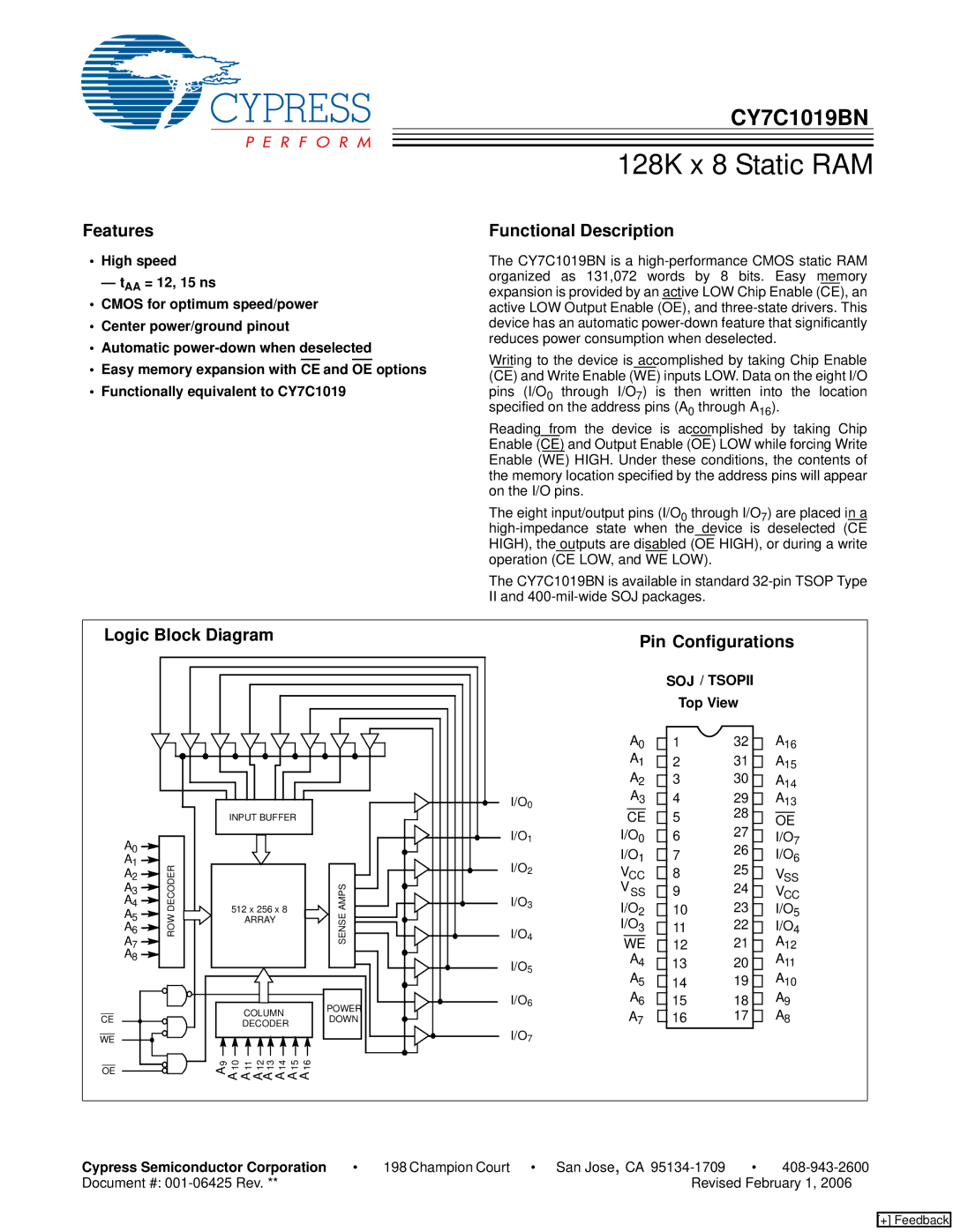
Logic Block Diagram |
|
|
|
| Pin Configurations | ||||||
|
|
|
|
|
|
|
| ||||
|
|
|
|
|
|
|
|
| SOJ / TSOPII |
| |
|
|
|
|
|
|
|
|
| Top View |
| |
|
|
|
|
|
|
|
| A0 | 1 | 32 | A16 |
|
|
|
|
|
|
|
| A1 | 2 | 31 | A15 |
|
|
|
|
|
|
|
| A2 | 3 | 30 | A |
|
|
|
|
|
|
|
| A3 |
|
| 14 |
|
|
|
|
|
|
| I/O0 | 4 | 29 | A | |
|
|
|
|
|
|
| CE | 5 | 28 | 13 | |
|
| INPUT BUFFER |
|
|
|
| OE | ||||
|
|
|
|
|
|
| I/O1 | I/O0 | 6 | 27 | I/O |
A0 |
|
|
|
|
|
|
|
|
| 26 | 7 |
|
|
|
|
|
|
| I/O1 | 7 | I/O6 | ||
A1 | DECODER |
|
|
|
|
| I/O2 | 25 | |||
A2 |
|
|
|
|
| VCC | 8 | V | |||
A3 |
|
|
| AMPS |
|
| VSS |
| 24 | SS | |
|
|
|
| I/O3 | 9 | VCC | |||||
A4 | 512 x 256 x 8 |
|
| I/O2 | 10 | 23 | I/O5 | ||||
A5 |
|
|
| ||||||||
ROW |
| ARRAY |
| SENSE |
|
| I/O3 |
| 22 | I/O4 | |
A6 |
|
|
|
| I/O4 | 11 | |||||
A7 |
|
|
|
|
|
|
| WE | 12 | 21 | A12 |
A8 |
|
|
|
|
|
| I/O5 | A4 | 13 | 20 | A11 |
|
|
|
|
|
|
|
| A5 | 14 | 19 | A10 |
|
|
|
| POWER |
| I/O6 | A6 | 15 | 18 | A9 | |
|
|
| COLUMN |
|
| A7 | 16 | 17 | A8 | ||
CE |
|
|
| DOWN |
|
| |||||
|
| DECODER |
|
| I/O7 | ||||||
WE |
|
|
|
|
|
|
|
|
|
| |
OE | 9 | 10 | 11 12 13 14 15 16 |
|
|
|
|
|
|
|
|
A A A A A A A A |
|
|
|
|
|
|
|
| |||
|
|
|
|
|
|
|
|
| |||
Cypress Semiconductor Corporation | • | 198 Champion Court | • | San Jose, CA | • | ||||||
Document #: |
|
|
|
|
| Revised February 1, 2006 | |||||
[+] Feedback