CY7C1019BN
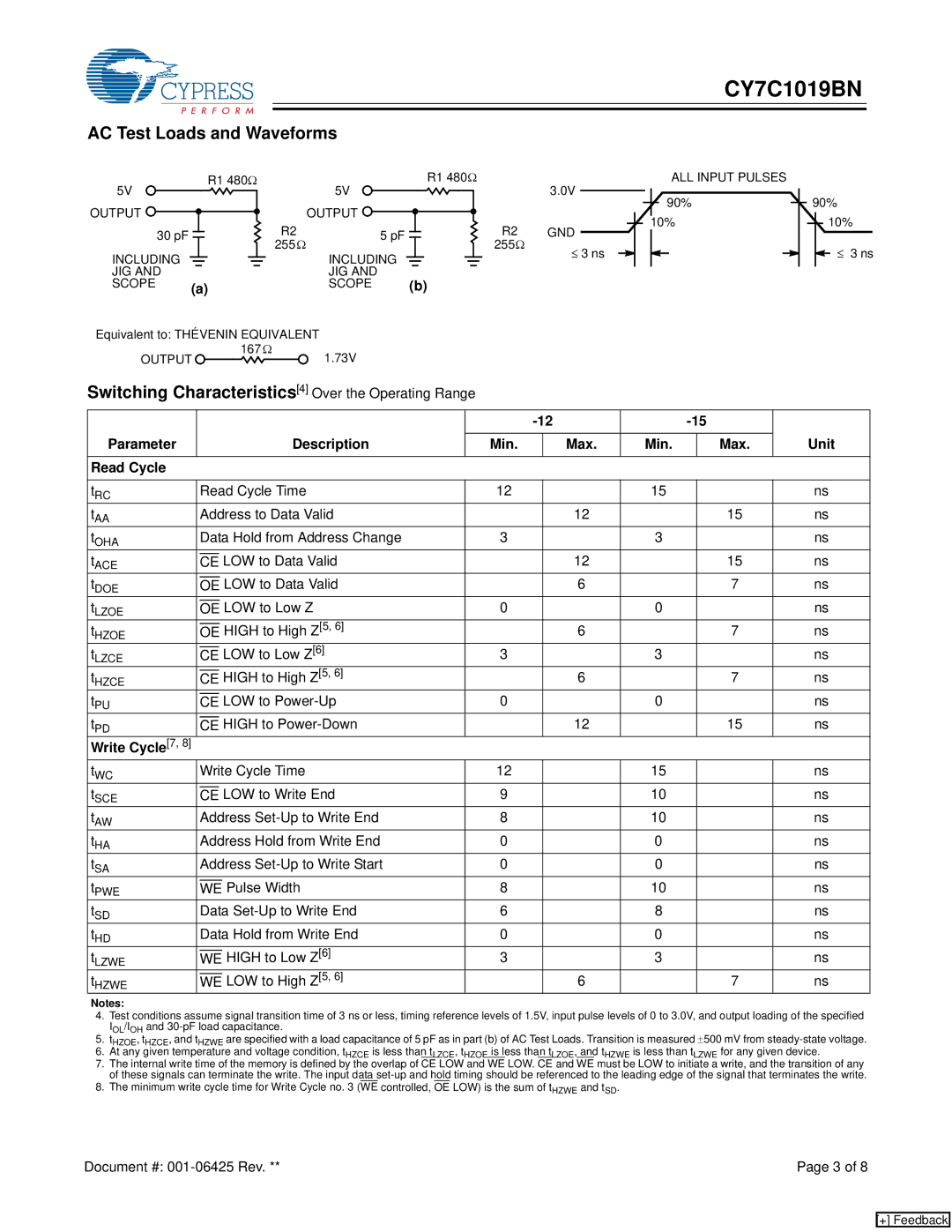
AC Test Loads and Waveforms
R1 480Ω |
5V |
OUTPUT |
30 pF ![]()
INCLUDING
JIG AND
SCOPE (a)
5V | R1 480Ω |
3.0V | |
OUTPUT |
|
R2 | 5 pF |
|
|
|
|
|
|
|
|
|
|
|
| R2 | GND |
| |
|
|
|
|
| |||||||||||||
255Ω |
|
|
|
|
|
|
|
|
|
|
|
|
|
| 255Ω | ≤ 3 ns | |
|
|
|
|
|
|
|
|
|
|
|
|
|
| ||||
|
|
|
|
|
|
|
|
|
|
|
|
|
|
|
| ||
| INCLUDING |
|
|
|
|
|
|
|
|
|
|
|
|
|
|
| |
|
|
|
|
|
|
|
|
|
|
|
|
|
|
|
| ||
| JIG AND | (b) |
|
| |||||||||||||
| SCOPE |
|
| ||||||||||||||
ALL INPUT PULSES
90%
10%
90%
10%
![]() ≤ 3 ns
≤ 3 ns
Equivalent to: THÉVENIN EQUIVALENT |
| ||||
OUTPUT | 167Ω | 1.73V | |||
|
|
|
| ||
Switching Characteristics[4] Over the Operating Range
|
|
|
|
|
|
|
|
| ||||
Parameter |
|
|
|
| Description |
|
|
|
|
| Unit | |
|
|
|
| Min. |
| Max. | Min. |
| Max. | |||
|
|
|
|
|
|
|
|
|
|
|
|
|
Read Cycle |
|
|
|
|
|
|
|
|
|
|
| |
|
|
|
|
|
|
|
|
| ||||
tRC |
| Read Cycle Time | 12 |
|
| 15 |
|
| ns | |||
tAA |
| Address to Data Valid |
|
| 12 |
|
| 15 | ns | |||
tOHA |
| Data Hold from Address Change | 3 |
|
| 3 |
|
| ns | |||
tACE |
|
|
| LOW to Data Valid |
|
| 12 |
|
| 15 | ns | |
CE |
|
|
| |||||||||
tDOE |
|
|
| LOW to Data Valid |
|
| 6 |
|
| 7 | ns | |
OE |
|
|
| |||||||||
tLZOE |
|
|
| LOW to Low Z | 0 |
|
| 0 |
|
| ns | |
OE |
|
|
| |||||||||
tHZOE |
|
|
| HIGH to High Z[5, 6] |
|
| 6 |
|
| 7 | ns | |
OE |
|
|
| |||||||||
tLZCE |
|
| LOW to Low Z[6] | 3 |
|
| 3 |
|
| ns | ||
CE |
|
|
| |||||||||
t |
|
|
|
| HIGH to High Z[5, 6] |
|
| 6 |
|
| 7 | ns |
CE |
|
|
| |||||||||
HZCE |
|
|
|
|
|
|
|
|
| |||
tPU |
|
| LOW to | 0 |
|
| 0 |
|
| ns | ||
CE |
|
|
| |||||||||
tPD |
|
| HIGH to |
|
| 12 |
|
| 15 | ns | ||
CE |
|
|
| |||||||||
Write Cycle[7, 8] |
|
|
|
|
|
|
|
|
|
|
|
|
tWC |
| Write Cycle Time | 12 |
|
| 15 |
|
| ns | |||
tSCE |
|
| LOW to Write End | 9 |
|
| 10 |
|
| ns | ||
CE |
|
|
| |||||||||
tAW |
| Address | 8 |
|
| 10 |
|
| ns | |||
tHA |
| Address Hold from Write End | 0 |
|
| 0 |
|
| ns | |||
tSA |
| Address | 0 |
|
| 0 |
|
| ns | |||
tPWE |
|
|
|
| Pulse Width | 8 |
|
| 10 |
|
| ns |
WE |
|
|
| |||||||||
tSD |
| Data | 6 |
|
| 8 |
|
| ns | |||
tHD |
| Data Hold from Write End | 0 |
|
| 0 |
|
| ns | |||
t |
|
|
|
| HIGH to Low Z[6] | 3 |
|
| 3 |
|
| ns |
WE |
|
|
| |||||||||
LZWE |
|
|
|
|
|
|
|
|
| |||
t |
|
|
|
| LOW to High Z[5, 6] |
|
| 6 |
|
| 7 | ns |
WE |
|
|
| |||||||||
HZWE |
|
|
|
|
|
|
|
|
| |||
Notes:
4.Test conditions assume signal transition time of 3 ns or less, timing reference levels of 1.5V, input pulse levels of 0 to 3.0V, and output loading of the specified IOL/IOH and
5.tHZOE, tHZCE, and tHZWE are specified with a load capacitance of 5 pF as in part (b) of AC Test Loads. Transition is measured ±500 mV from
6.At any given temperature and voltage condition, tHZCE is less than tLZCE, tHZOE is less than tLZOE, and tHZWE is less than tLZWE for any given device.
7.The internal write time of the memory is defined by the overlap of CE LOW and WE LOW. CE and WE must be LOW to initiate a write, and the transition of any of these signals can terminate the write. The input data
8.The minimum write cycle time for Write Cycle no. 3 (WE controlled, OE LOW) is the sum of tHZWE and tSD.
Document #: | Page 3 of 8 |
[+] Feedback