CY7C1019BN
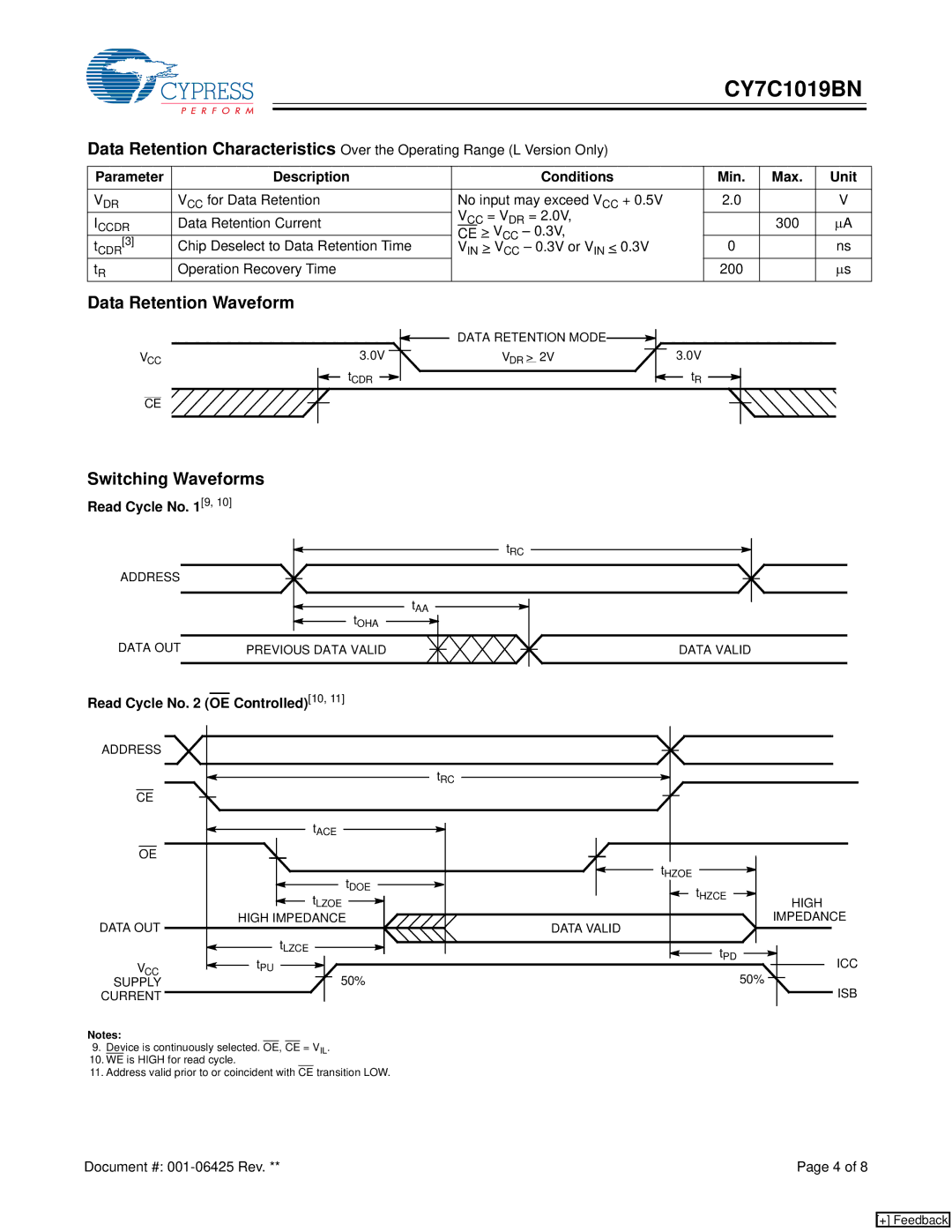
Data Retention Characteristics Over the Operating Range (L Version Only)
Parameter | Description | Conditions | Min. | Max. | Unit |
|
|
|
|
|
|
VDR | VCC for Data Retention | No input may exceed VCC + 0.5V | 2.0 |
| V |
|
| VCC = VDR = 2.0V, |
|
|
|
ICCDR | Data Retention Current |
| 300 | ∝A | |
CE > VCC – 0.3V, |
| ||||
tCDR[3] | Chip Deselect to Data Retention Time | 0 |
| ns | |
VIN > VCC – 0.3V or VIN < 0.3V |
| ||||
tR | Operation Recovery Time |
| 200 |
| ∝s |
Data Retention Waveform
|
| DATA RETENTION MODE |
|
VCC | 3.0V | VDR > 2V | 3.0V |
| tCDR |
| tR |
CE |
|
|
|
Switching Waveforms
Read Cycle No. 1[9, 10]
tRC
ADDRESS
tAA
tOHA
DATA OUT | PREVIOUS DATA VALID |
DATA VALID
Read Cycle No. 2 (OE Controlled)[10, 11] |
|
| |
ADDRESS |
|
|
|
|
| tRC |
|
CE |
|
|
|
| tACE |
|
|
OE |
| tHZOE |
|
| tDOE |
| |
| tHZCE |
| |
| tLZOE | HIGH | |
DATA OUT | HIGH IMPEDANCE | DATA VALID | IMPEDANCE |
|
| ||
| tLZCE | tPD |
|
VCC | tPU | ICC | |
SUPPLY | 50% |
| 50% |
CURRENT |
|
| ISB |
Notes:
9.Device is continuously selected. OE, CE = VIL.
10. WE is HIGH for read cycle.
11. Address valid prior to or coincident with CE transition LOW.
Document #: | Page 4 of 8 |
[+] Feedback