Manuals
/
Cypress
/
Computer Equipment
/
Computer Hardware
Cypress
CY7C1019CV33
manual
Pin Tsop II
Models:
CY7C1019CV33
1
8
10
10
Download
10 pages
62.17 Kb
3
4
5
6
7
8
9
10
Logic Block Diagram
0-I/O Mode Power
Switching Waveforms
Page 8
Image 8
CY7C1019CV33
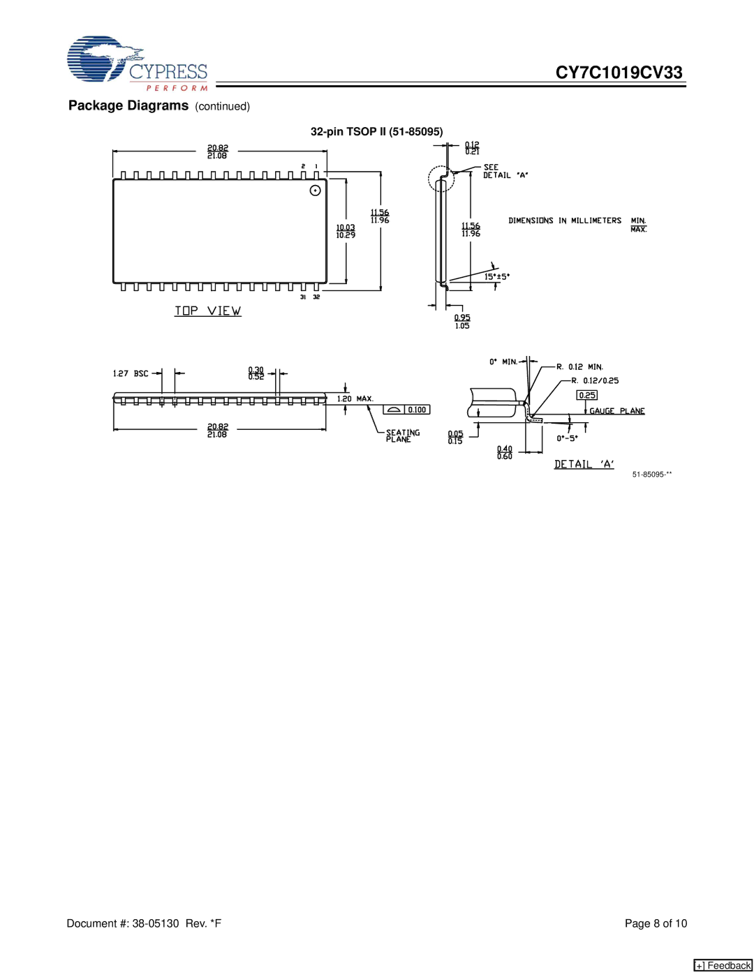
Package Diagrams
(continued)
32-pin
TSOP II
(51-85095)
51-85095-**
Document #:
38-05130
Rev. *F
Page 8 of 10
[+] Feedback
Page 7
Page 9
Page 8
Image 8
Page 7
Page 9
Contents
Features
Logic Block Diagram
Pin Configuration
Functional Description
Unit
Pin Configuration1 Selection Guide
Ball Vfbga Top View
Electrical Characteristics Over the Operating Range
Maximum Ratings
Operating Range
Capacitance3
Switching Characteristics Over the Operating Range5
AC Test Loads and Waveforms4
Parameter Description Unit Min Max Read Cycle
Write Cycle 9
Switching Waveforms
Read Cycle No
Read Cycle No OE Controlled 12
Write Cycle No CE Controlled14
0-I/O Mode Power
Truth Table
Write Cycle No WE Controlled, OE High During Write14
Write Cycle No WE Controlled, OE LOW15
Pin 400-Mil Molded SOJ
Package Diagrams
Ordering Information
Pin Tsop II
Ball Vfbga 6 x 8 x 1 mm
Issue Orig. Description of Change Date
Document History
Top
Page
Image
Contents