Manuals
/
Cypress
/
Computer Equipment
/
Computer Hardware
Cypress
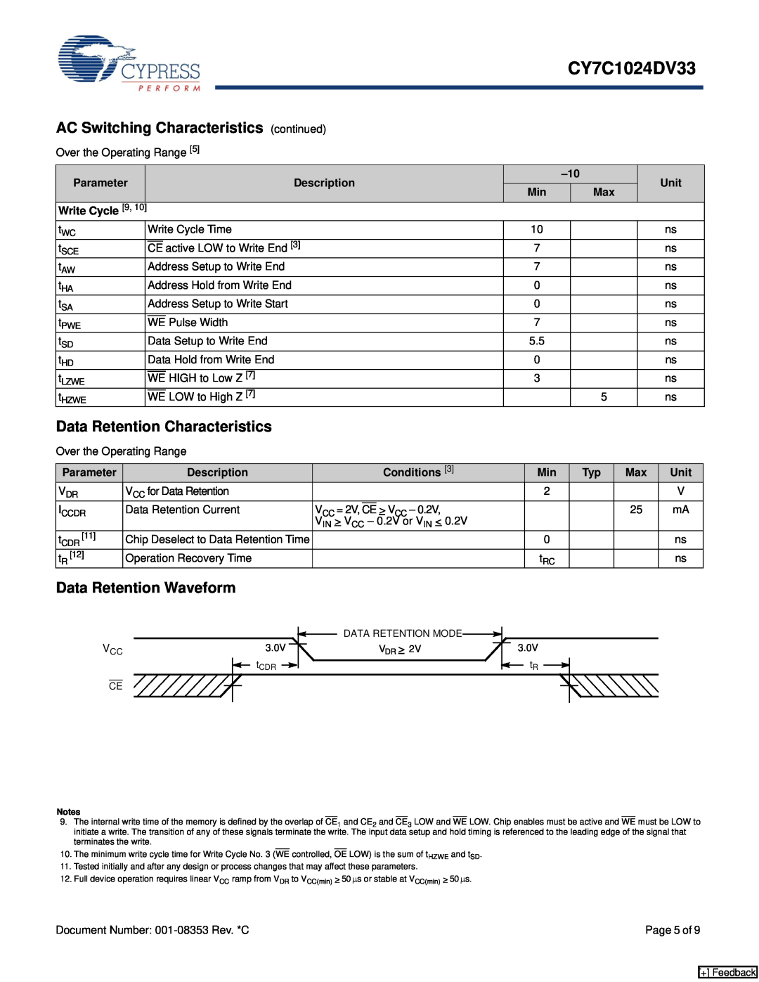
CY7C1024DV33 AC Switching Characteristics continued, Data Retention Characteristics, Unit
Models:
CY7C1024DV33
1
5
9
9
Download
9 pages
54.03 Kb
1
2
3
4
5
6
7
8
DC Electrical Characteristics
Logic Block Diagram
Pin Configuration
Power
PSoC Solutions
AC Switching Characteristics
Page 5
Image 5
Page 4
Page 6
Page 5
Image 5
Page 4
Page 6
Contents
Logic Block Diagram
Features
CY7C1024DV33
Functional Description
Selection Guide
Pin Configuration
Description
Unit
Maximum Ratings
DC Electrical Characteristics
Operating Range
Capacitance
Parameter Read Cycle
AC Switching Characteristics
Figure 2. AC Test Loads and Waveform4
Data Retention Characteristics
AC Switching Characteristics continued
Data Retention Waveform
Conditions
Figure 3. Read Cycle No. 1 Address Transition Controlled 13
Switching Waveforms
Figure 4. Read Cycle No. 2 OE Controlled 3, 14
Figure 5. Write Cycle No. 1 CE Controlled 3, 16
Power
Switching Waveforms continued
Truth Table
Figure 6. Write Cycle No. 2 WE Controlled, OE HIGH During Write 3, 16
Ordering Information
Package Diagram
Speed
Ordering Code
Document History Page
Sales, Solutions, and Legal Information
Document Title CY7C1024DV33, 3-Mbit 128K X 24 Static RAM
Document Number
Top
Page
Image
Contents