CY7C1166V18, CY7C1177V18 CY7C1168V18, CY7C1170V18
echo clock and follows the timing of any data pin. This signal is asserted half a cycle before valid data arrives.
DLL
These chips use a Delay Lock Loop (DLL) that is designed to function between 120 MHz and the specified maximum clock frequency. The DLL may be disabled by applying ground to the DOFF pin. When the DLL is turned off, the device behaves in
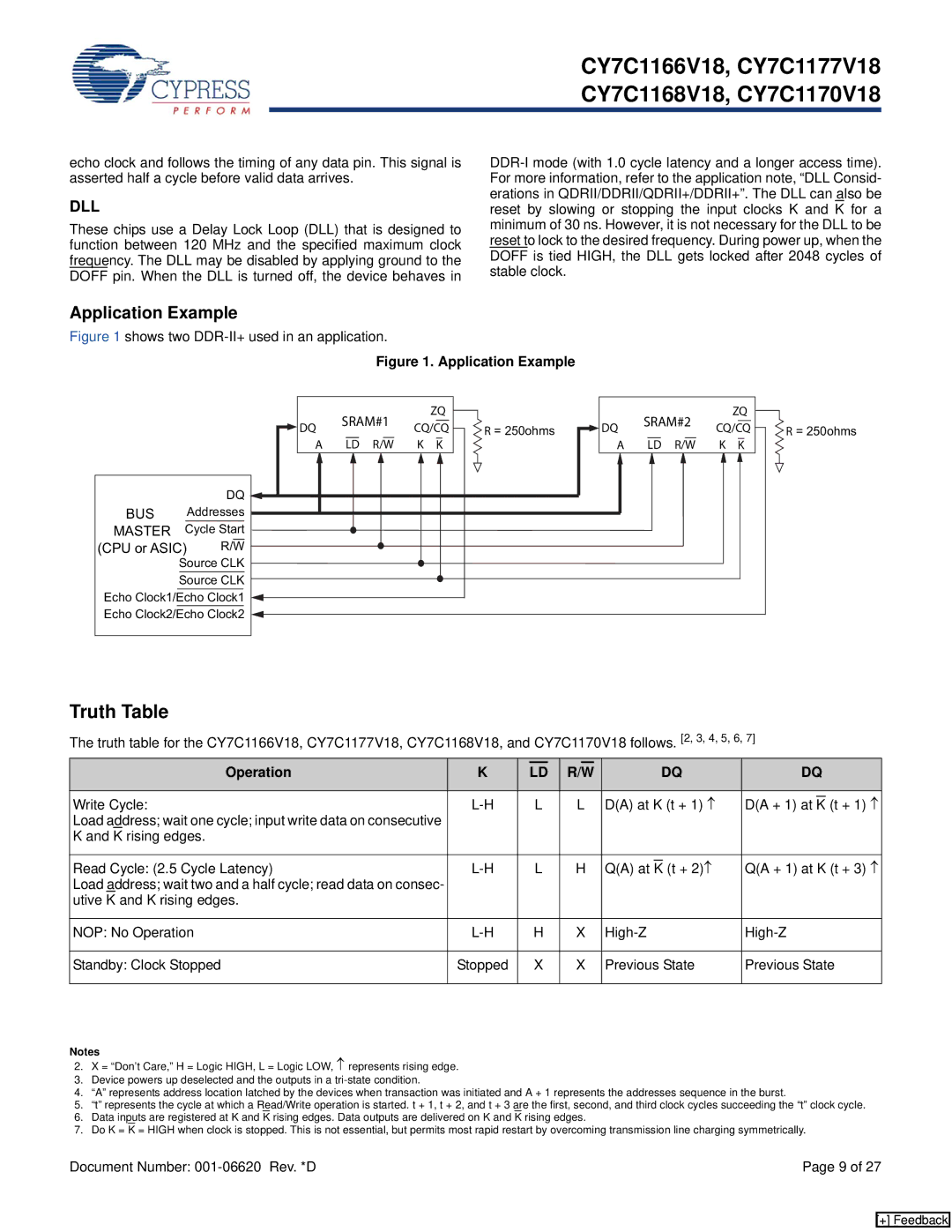
Application Example
Figure 1 shows two DDR-II+ used in an application.
Figure 1. Application Example
|
|
| SRAM#1 |
| ZQ |
|
| SRAM#2 |
| ZQ |
| ||
|
| DQ | CQ/CQ | R = 250ohms | DQ | CQ/CQ | R = 250ohms | ||||||
|
|
|
|
|
| ||||||||
|
| A | LD | R/W | K | K |
| A | LD | R/W | K | K |
|
|
| DQ |
|
|
|
|
|
|
|
|
|
|
|
BUS |
| Addresses |
|
|
|
|
|
|
|
|
|
|
|
MASTER | Cycle Start |
|
|
|
|
|
|
|
|
|
|
| |
(CPU or ASIC) | R/W |
|
|
|
|
|
|
|
|
|
|
| |
| Source CLK |
|
|
|
|
|
|
|
|
|
|
| |
| Source CLK |
|
|
|
|
|
|
|
|
|
|
| |
Echo Clock1/Echo Clock1 |
|
|
|
|
|
|
|
|
|
|
| ||
Echo Clock2/Echo Clock2 |
|
|
|
|
|
|
|
|
|
|
| ||
Truth Table
The truth table for the CY7C1166V18, CY7C1177V18, CY7C1168V18, and CY7C1170V18 follows. [2, 3, 4, 5, 6, 7]
Operation | K |
| LD | R/W |
| DQ | DQ | ||||||
|
|
|
|
|
|
|
|
|
|
|
|
|
|
Write Cycle: |
| L | L | D(A) at K (t + 1) ↑ | D(A + 1) at |
| (t + 1) ↑ | ||||||
K | |||||||||||||
Load address; wait one cycle; input write data on consecutive |
|
|
|
|
|
|
|
|
|
|
|
|
|
K and K rising edges. |
|
|
|
|
|
|
|
|
|
|
|
|
|
|
|
|
|
|
|
|
|
| |||||
Read Cycle: (2.5 Cycle Latency) |
| L | H | Q(A) at |
| (t + 2)↑ | Q(A + 1) at K (t + 3) ↑ | ||||||
K | |||||||||||||
Load address; wait two and a half cycle; read data on consec- |
|
|
|
|
|
|
|
|
|
|
|
|
|
utive K and K rising edges. |
|
|
|
|
|
|
|
|
|
|
|
|
|
|
|
|
|
|
|
| |||||||
NOP: No Operation |
| H | X | ||||||||||
|
|
|
|
|
|
| |||||||
Standby: Clock Stopped | Stopped |
| X | X | Previous State | Previous State | |||||||
|
|
|
|
|
|
|
|
|
|
|
|
|
|
Notes
2.X = “Don’t Care,” H = Logic HIGH, L = Logic LOW, ↑ represents rising edge.
3.Device powers up deselected and the outputs in a
4.“A” represents address location latched by the devices when transaction was initiated and A + 1 represents the addresses sequence in the burst.
5.“t” represents the cycle at which a Read/Write operation is started. t + 1, t + 2, and t + 3 are the first, second, and third clock cycles succeeding the “t” clock cycle.
6.Data inputs are registered at K and K rising edges. Data outputs are delivered on K and K rising edges.
7.Do K = K = HIGH when clock is stopped. This is not essential, but permits most rapid restart by overcoming transmission line charging symmetrically.
Document Number: | Page 9 of 27 |
[+] Feedback