
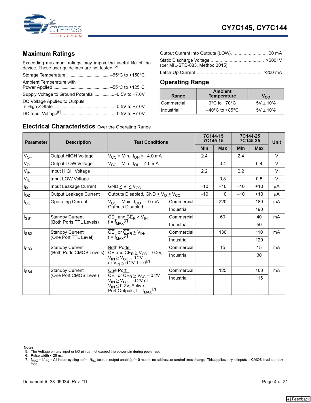
CY7C145, CY7C144 specifications
Cypress Semiconductor is renowned for its advanced memory solutions, and two of its noteworthy products are the CY7C144 and CY7C145, both of which serve as emerging leaders in the field of synchronous dynamic random-access memory (SDRAM). These memory chips provide high-speed data access, making them ideal for various applications, including networking, automotive, and industrial electronics.The CY7C144 is a 4-Mbit SRAM, while its counterpart, the CY7C145, is an 8-Mbit SRAM. Both chips utilize a synchronous interface, which allows them to operate at clock rates that significantly enhance data retrieval speeds. Designed for low power consumption, these devices feature several power-saving modes, making them suitable for battery-operated applications.
One of the main features of the CY7C144 and CY7C145 is their support for burst read and write operations. This function enables the memory to deliver multiple bits of data sequentially with a single command, substantially increasing throughput. Additionally, both models come with a wide data bus, typically 16 bits, allowing for efficient data handling and alignment with a variety of systems.
The technology behind these chips includes static CMOS processes, which promote high performance and reliability under various operating environments. The CY7C144 and CY7C145 both guarantee a high level of data integrity, thanks to advanced error detection and correction features. This makes them especially valuable in applications where data accuracy is critical.
Another critical aspect is the integration of an on-chip address decoder for efficient memory addressing, minimizing delays during data access. This characteristic plays a crucial role in optimizing the overall system performance, particularly in high-bandwidth applications.
In terms of environmental resilience, these memories are designed to withstand a range of temperatures, making them robust enough for industrial applications. The CY7C144 and CY7C145 also comply with several industry standards, ensuring compatibility with a wide array of devices and systems.
In summary, the CY7C144 and CY7C145 by Cypress Semiconductor stand out due to their blend of high speed, low power consumption, and robust reliability. With advanced features like burst read/write capabilities, error detection, and temperature resilience, these memory chips are exceptional choices for modern electronic applications demanding speed and efficiency. Their continued evolution reflects Cypress's commitment to innovation in the semiconductor industry, catering to the growing needs of a data-driven world.