CY7C68023/CY7C68024
3.0Pin Assignments
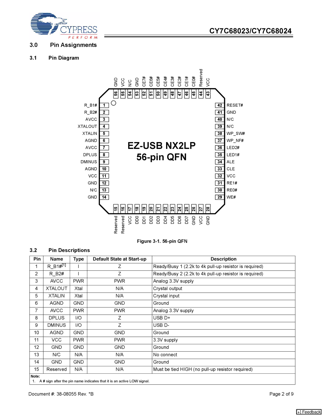
3.1Pin Diagram
R_B1#
R_B2#
AVCC XTALOUT XTALIN AGND AVCC DPLUS DMINUS AGND VCC GND N/C
GND
1
2
3
4
5
6
7
8
9
10
11
12
13
14
GND |
| VCC |
| N/C |
| GND |
| CE7# |
| CE6# |
| CE5# |
| CE4# |
| CE3# |
| CE2# |
| CE1# |
| CE0# |
| Reserved |
| VCC |
|
|
|
|
|
|
|
|
|
|
|
|
|
|
|
|
|
|
|
|
|
|
|
|
|
|
|
56 |
| 55 |
| 54 |
| 53 |
| 52 |
| 51 |
| 50 |
| 49 |
| 48 |
| 47 |
| 46 |
| 45 |
| 44 |
| 43 |
|
|
|
|
|
|
|
|
|
|
|
|
|
|
|
|
|
|
|
|
|
|
|
|
|
|
|
EZ-USB NX2LP
56-pin QFN
| 15 |
| 16 |
| 17 |
| 18 |
| 19 |
| 20 |
| 21 |
| 22 |
| 23 |
| 24 |
| 25 |
| 26 |
| 27 |
| 28 |
|
|
|
|
|
|
|
|
|
|
|
|
|
|
|
|
|
|
|
|
|
|
|
|
|
|
|
|
|
|
| Reserved |
| Reserved |
| VCC |
| DD0 |
| DD1 |
| DD2 |
| DD3 |
| DD4 |
| DD5 |
| DD6 |
| DD7 |
| GND |
| VCC |
| GND |
|
|
|
|
|
|
|
|
|
|
|
|
|
|
|
|
|
|
|
|
|
|
|
|
|
|
|
|
|
|
42
41
40
39
38
37
36
35
34
33
32
31
30
29
RESET# GND N/C N/C WP_SW# WP_NF# LED2# LED1#
ALE
CLE
VCC
RE1#
RE0#
WE#
Figure 3-1. 56-pin QFN
3.2Pin Descriptions
| Pin | Name | Type | Default State at | Description |
| 1 | R_B1#[1] | I | Z | Ready/Busy 1 (2.2k to 4k |
| 2 | R_B2# | I | Z | Ready/Busy 2 (2.2k to 4k |
|
|
|
|
|
|
| 3 | AVCC | PWR | PWR | Analog 3.3V supply |
|
|
|
|
|
|
| 4 | XTALOUT | Xtal | N/A | Crystal output |
|
|
|
|
|
|
| 5 | XTALIN | Xtal | N/A | Crystal input |
|
|
|
|
|
|
| 6 | AGND | GND | GND | Ground |
|
|
|
|
|
|
| 7 | AVCC | PWR | PWR | Analog 3.3V supply |
|
|
|
|
|
|
| 8 | DPLUS | I/O | Z | USB D+ |
|
|
|
|
|
|
| 9 | DMINUS | I/O | Z | USB D- |
|
|
|
|
|
|
| 10 | AGND | GND | GND | Ground |
|
|
|
|
|
|
| 11 | VCC | PWR | PWR | 3.3V supply |
|
|
|
|
|
|
| 12 | GND | GND | GND | Ground |
|
|
|
|
|
|
| 13 | N/C | N/A | N/A | No connect |
|
|
|
|
|
|
| 14 | GND | GND | GND | Ground |
|
|
|
|
|
|
| 15 | Reserved | N/A | N/A | Must be tied HIGH (no |
|
|
|
|
|
|
| Note: |
|
|
|
|
| 1. A # sign after the pin name indicates that it is an active LOW signal. |
| |||
|
|
|
|
|
|
Document #: | Page 2 of 9 | ||||
[+] Feedback