FS781/82/84
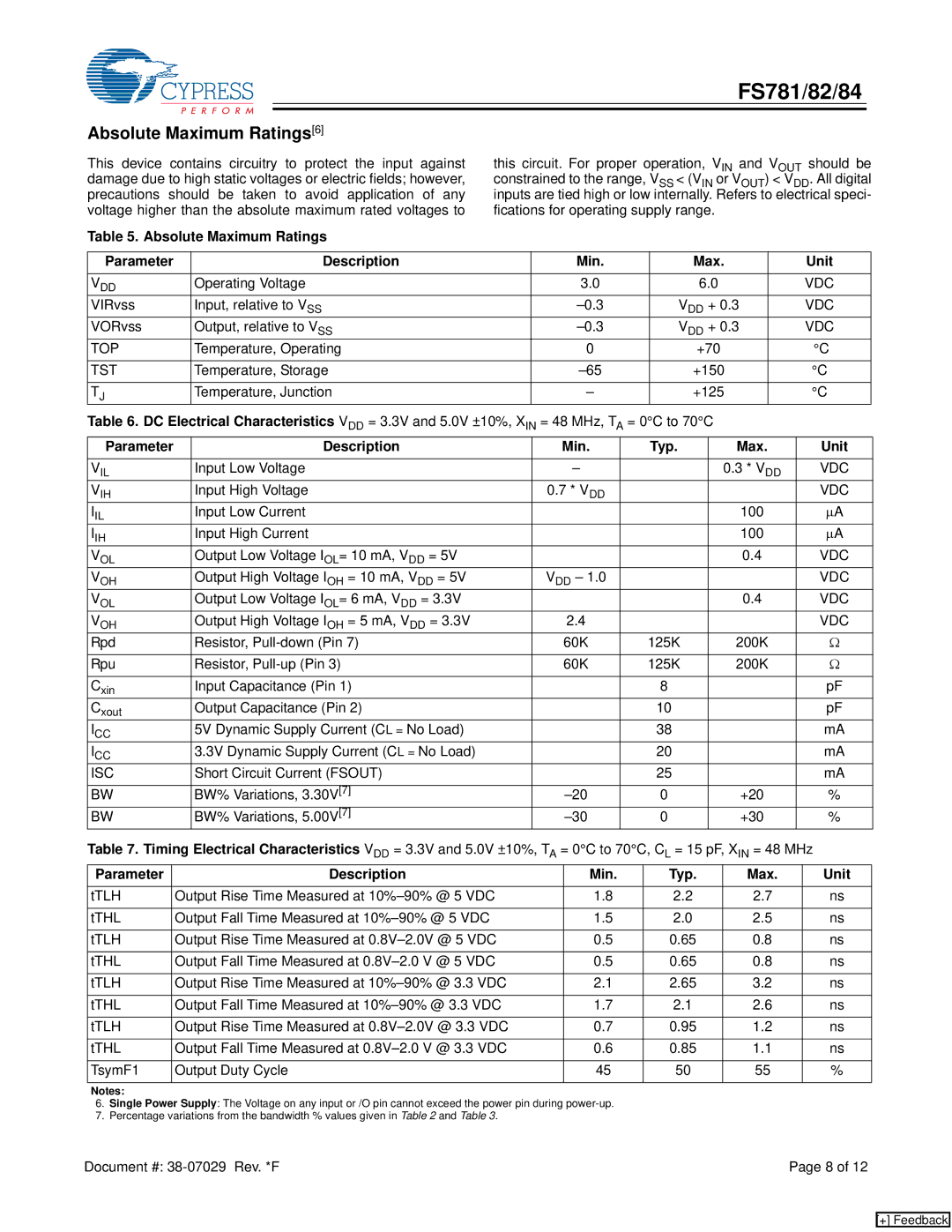
Absolute Maximum Ratings[6]
This device contains circuitry to protect the input against damage due to high static voltages or electric fields; however, precautions should be taken to avoid application of any voltage higher than the absolute maximum rated voltages to
this circuit. For proper operation, VIN and VOUT should be constrained to the range, VSS < (VIN or VOUT) < VDD. All digital inputs are tied high or low internally. Refers to electrical speci- fications for operating supply range.
Table 5. Absolute Maximum Ratings
Parameter | Description | Min. |
|
| Max. |
| Unit | |
VDD | Operating Voltage | 3.0 |
|
| 6.0 |
| VDC | |
VIRvss | Input, relative to VSS |
| VDD + 0.3 |
| VDC | |||
VORvss | Output, relative to VSS |
| VDD + 0.3 |
| VDC | |||
TOP | Temperature, Operating | 0 |
|
| +70 |
| °C | |
|
|
|
|
|
|
|
|
|
TST | Temperature, Storage |
|
| +150 |
| °C | ||
|
|
|
|
|
|
|
|
|
TJ | Temperature, Junction | – |
|
| +125 |
| °C | |
Table 6. DC Electrical Characteristics VDD = 3.3V and 5.0V ±10%, XIN = 48 MHz, TA = 0°C to 70°C |
| |||||||
Parameter | Description | Min. |
| Typ. |
| Max. | Unit | |
|
|
|
|
|
|
|
| |
VIL | Input Low Voltage | – |
|
|
| 0.3 * VDD | VDC | |
VIH | Input High Voltage | 0.7 * VDD |
|
|
|
|
| VDC |
IIL | Input Low Current |
|
|
|
| 100 |
| ∝A |
IIH | Input High Current |
|
|
|
| 100 |
| ∝A |
VOL | Output Low Voltage IOL= 10 mA, VDD = 5V |
|
|
|
| 0.4 |
| VDC |
VOH | Output High Voltage IOH = 10 mA, VDD = 5V | VDD – 1.0 |
|
|
|
|
| VDC |
VOL | Output Low Voltage IOL= 6 mA, VDD = 3.3V |
|
|
|
| 0.4 |
| VDC |
VOH | Output High Voltage IOH = 5 mA, VDD = 3.3V | 2.4 |
|
|
|
|
| VDC |
Rpd | Resistor, | 60K | 125K |
| 200K | Ω | ||
|
|
|
|
|
|
| ||
Rpu | Resistor, | 60K | 125K |
| 200K | Ω | ||
|
|
|
|
|
|
|
| |
Cxin | Input Capacitance (Pin 1) |
| 8 |
|
|
| pF | |
Cxout | Output Capacitance (Pin 2) |
| 10 |
|
|
| pF | |
ICC | 5V Dynamic Supply Current (CL = No Load) |
| 38 |
|
|
| mA | |
ICC | 3.3V Dynamic Supply Current (CL = No Load) |
| 20 |
|
|
| mA | |
ISC | Short Circuit Current (FSOUT) |
| 25 |
|
|
| mA | |
|
|
|
|
|
|
|
| |
BW | BW% Variations, 3.30V[7] | 0 |
| +20 |
| % | ||
BW | BW% Variations, 5.00V[7] | 0 |
| +30 |
| % | ||
Table 7. Timing Electrical Characteristics VDD = 3.3V and 5.0V ±10%, TA = 0°C to 70°C, CL = 15 pF, XIN = 48 MHz
Parameter | Description | Min. | Typ. | Max. | Unit |
tTLH | Output Rise Time Measured at | 1.8 | 2.2 | 2.7 | ns |
|
|
|
|
|
|
tTHL | Output Fall Time Measured at | 1.5 | 2.0 | 2.5 | ns |
|
|
|
|
|
|
tTLH | Output Rise Time Measured at | 0.5 | 0.65 | 0.8 | ns |
|
|
|
|
|
|
tTHL | Output Fall Time Measured at | 0.5 | 0.65 | 0.8 | ns |
|
|
|
|
|
|
tTLH | Output Rise Time Measured at | 2.1 | 2.65 | 3.2 | ns |
|
|
|
|
|
|
tTHL | Output Fall Time Measured at | 1.7 | 2.1 | 2.6 | ns |
|
|
|
|
|
|
tTLH | Output Rise Time Measured at | 0.7 | 0.95 | 1.2 | ns |
|
|
|
|
|
|
tTHL | Output Fall Time Measured at | 0.6 | 0.85 | 1.1 | ns |
|
|
|
|
|
|
TsymF1 | Output Duty Cycle | 45 | 50 | 55 | % |
|
|
|
|
|
|
Notes:
6.Single Power Supply: The Voltage on any input or /O pin cannot exceed the power pin during
7.Percentage variations from the bandwidth % values given in Table 2 and Table 3.
Document #: | Page 8 of 12 |
[+] Feedback