|
|
|
|
|
|
|
|
|
|
|
| FS781/82/84 | ||
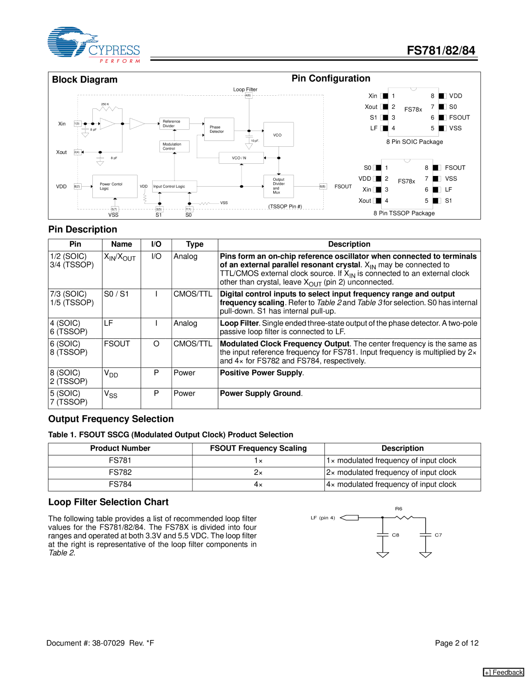
Block Diagram |
|
|
|
| Loop Filter | Pin Configuration |
|
|
|
| ||||
|
|
|
|
|
|
|
|
| Xin | 1 |
| 8 | VDD | |
|
|
|
|
|
|
| 4(6) |
|
|
| ||||
|
|
|
|
|
|
|
|
|
|
| ||||
|
| 250 K |
|
|
|
|
|
|
| Xout | 2 | FS78x | 7 | S0 |
|
|
|
|
|
|
|
|
|
| |||||
|
|
|
|
|
|
|
|
|
|
|
|
|
| |
Xin |
|
|
| Reference |
|
|
|
|
| S1 | 3 |
| 6 | FSOUT |
1(3) |
|
|
|
|
|
|
|
|
|
|
|
| ||
|
| Divider |
| Phase |
|
|
| LF | 4 |
| 5 | VSS | ||
| 8 pF |
|
|
|
|
|
| |||||||
|
|
|
|
|
|
|
|
| ||||||
|
|
|
|
| Detector |
|
|
|
| |||||
|
|
|
|
|
| VCO |
|
|
|
|
|
|
| |
|
|
|
|
|
|
|
|
|
|
|
|
|
| |
|
|
|
| Modulation |
|
| 10 pF. |
|
|
| 8 Pin SOIC Package |
| ||
|
|
|
|
|
|
|
|
|
|
| ||||
Xout | 2(4) |
|
| Control |
|
|
|
|
|
|
|
|
|
|
|
|
|
|
| VCO / N |
|
|
|
|
|
|
| ||
|
| 8 pF |
|
|
|
|
|
|
|
|
|
|
| |
|
|
|
|
|
|
|
|
|
| S0 | 1 |
| 8 | FSOUT |
|
|
|
|
|
|
| Output |
|
| VDD | 2 | FS78x | 7 | VSS |
VDD | 8(2) | Power Contol | VDD | Input Control Logic |
|
| Divider | 6(8) | FSOUT | Xin | 3 | 6 | LF | |
Logic |
|
| and |
| ||||||||||
|
|
|
|
|
|
|
|
| ||||||
|
|
|
|
|
|
| Mux |
|
|
|
|
|
|
|
|
|
|
|
|
| VSS | (TSSOP Pin #) |
| Xout | 4 |
| 5 | S1 | |
|
| 5(7) |
| 3(5) | 7(1) |
|
| 8 Pin TSSOP Package |
| |||||
|
|
|
|
|
|
|
| |||||||
|
| VSS |
| S1 | S0 |
|
|
|
|
| ||||
Pin Description
| Pin | Name | I/O | Type | Description |
1/2 (SOIC) | XIN/XOUT | I/O | Analog | Pins form an | |
3/4 (TSSOP) |
|
|
| of an external parallel resonant crystal. XIN may be connected to | |
|
|
|
|
| TTL/CMOS external clock source. If XIN is connected to an external clock |
|
|
|
|
| other than crystal, leave XOUT (pin 2) unconnected. |
7/3 (SOIC) | S0 / S1 | I | CMOS/TTL | Digital control inputs to select input frequency range and output | |
1/5 (TSSOP) |
|
|
| frequency scaling. Refer to Table 2 and Table 3 for selection. S0 has internal | |
|
|
|
|
| |
4 | (SOIC) | LF | I | Analog | Loop Filter. Single ended |
6 | (TSSOP) |
|
|
| passive loop filter is connected to LF. |
6 | (SOIC) | FSOUT | O | CMOS/TTL | Modulated Clock Frequency Output. The center frequency is the same as |
8 | (TSSOP) |
|
|
| the input reference frequency for FS781. Input frequency is multiplied by 2× |
|
|
|
|
| and 4× for FS782 and FS784, respectively. |
8 | (SOIC) | VDD | P | Power | Positive Power Supply. |
2 | (TSSOP) |
|
|
|
|
5 | (SOIC) | VSS | P | Power | Power Supply Ground. |
7 | (TSSOP) |
|
|
|
|
Output Frequency Selection
Table 1. FSOUT SSCG (Modulated Output Clock) Product Selection
Product Number | FSOUT Frequency Scaling | Description |
FS781 | 1× | 1× modulated frequency of input clock |
|
|
|
FS782 | 2× | 2× modulated frequency of input clock |
|
|
|
FS784 | 4× | 4× modulated frequency of input clock |
|
|
|
Loop Filter Selection Chart
The following table provides a list of recommended loop filter values for the FS781/82/84. The FS78X is divided into four ranges and operated at both 3.3V and 5.5 VDC. The loop filter at the right is representative of the loop filter components in Table 2.
LF (pin 4)
R6
C8
C7
Document #: | Page 2 of 12 |
[+] Feedback