Z9973
3.3V, 125-MHz, Multi-Output Zero Delay Buffer
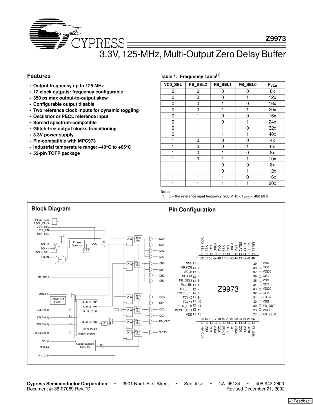
Features | Table 1. Frequency Table[1] |
|
| ||
• Output frequency up to 125 MHz | VC0_SEL | FB_SEL2 | FB_SEL1 | FB_SEL0 | FVC0 |
• 12 clock outputs: frequency configurable | 0 | 0 | 0 | 0 | 8x |
• 350 ps max | 0 | 0 | 0 | 1 | 12x |
• Configurable output disable | 0 | 0 | 1 | 0 | 16x |
• Two reference clock inputs for dynamic toggling | 0 | 0 | 1 | 1 | 20x |
• Oscillator or PECL reference input | 0 | 1 | 0 | 0 | 16x |
• Spread | 0 | 1 | 0 | 1 | 24x |
• | 0 | 1 | 1 | 0 | 32x |
• 3.3V power supply | 0 | 1 | 1 | 1 | 40x |
• | 1 | 0 | 0 | 0 | 4x |
• Industrial temperature range: | 1 | 0 | 0 | 1 | 6x |
• | 1 | 0 | 1 | 0 | 8x |
| 1 | 0 | 1 | 1 | 10x |
| 1 | 1 | 0 | 0 | 8x |
| 1 | 1 | 0 | 1 | 12x |
| 1 | 1 | 1 | 0 | 16x |
| 1 | 1 | 1 | 1 | 20x |
| Note: |
|
|
|
|
| 1. x = the reference input frequency, 200 MHz < FVCO < 480 MHz. | ||||
| . |
|
|
|
|
|
|
|
| ||
Block Diagram | Pin Configuration |
|
| ||
PECL_CLK
PECL_CLK#
VCO_SEL
PLL_EN
REF_SEL
|
|
|
|
|
|
| D Q | Sync | QA0 |
|
|
|
|
|
|
| Frz | ||
|
| Phase |
|
| 0 |
|
|
| |
TCLK0 | 0 |
| VCO |
|
|
| QA1 | ||
Detector | 1 |
|
|
| |||||
|
|
|
|
| |||||
TCLK1 | 1 |
|
| LPF |
|
|
|
| QA2 |
TCLK_SEL |
|
|
|
|
|
|
| ||
|
|
|
|
|
|
|
|
| |
FB_IN |
|
|
|
|
|
|
|
| QA3 |
|
|
|
|
|
|
| D Q | Sync | QB0 |
|
|
|
|
|
|
| Frz | ||
|
|
|
|
|
|
|
|
| |
|
|
|
|
|
|
|
|
| QB1 |
FB_SEL2 |
|
|
|
|
|
|
|
| QB2 |
|
|
|
|
|
|
|
|
| |
|
|
|
|
|
|
|
|
| QB3 |
MR#/OE |
|
|
|
|
|
| D Q | Sync |
|
|
|
|
|
|
|
| QC0 | ||
|
|
|
|
|
| Frz | |||
|
|
|
|
|
|
|
| ||
| Reset |
| /4, /6, /8, /12 |
|
|
|
| QC1 | |
|
|
|
|
|
|
|
|
| |
| 2 |
| /4, /6, /8, /10 |
|
|
| Sync |
| |
SELA(0,1) |
|
| /2, /4, /6, /8 |
|
| D Q | QC2 | ||
|
|
|
|
| Frz | ||||
|
|
|
|
|
|
|
| ||
SELB(0,1) | 2 |
|
|
|
|
|
|
| QC3 |
|
|
|
|
|
|
|
| ||
|
|
|
|
| 0 |
| Sync |
| |
| 2 |
| /4, /6, /8, /10 |
| D Q | FB_OUT | |||
SELC(0,1) |
| /2 | 1 | Frz | |||||
|
|
|
|
| |||||
|
|
|
|
|
|
|
|
| |
|
|
|
| Sync Pulse |
|
|
| Sync |
|
FB_SEL(0,1) | 2 | Data Generator |
|
| D Q | SYNC | |||
|
| Frz | |||||||
|
|
|
|
|
| ||||
SCLK |
| Output Disable |
|
|
|
|
| ||
|
| 12 |
|
|
|
| |||
SDATA |
| Circuitry |
|
|
|
| |||
|
|
|
|
|
| ||||
INV_CLK |
|
|
|
|
|
|
|
|
|
VSS MR#/OE
SCLK
SDATA
FB_SEL2
PLL_EN
REF_SEL TCLK_SEL TCLK0 TCLK1
PECL_CLK PECL_CLK#
VDD
|
|
|
|
| VCO SEL | VSS | QA0 | VDDC | QA3 VDDC QA2 VSS QA1 | SELA0 | SELA1 | SELB0 | SELB1 |
|
| ||||||||||||||||||
|
|
|
|
|
|
|
|
|
|
|
|
|
|
|
|
|
|
|
|
|
|
|
|
|
|
|
|
|
|
|
|
| |
|
|
|
|
|
|
|
|
|
|
|
|
|
|
|
|
|
|
|
|
|
|
|
|
|
|
|
|
|
|
|
|
|
|
|
|
|
|
|
|
|
|
|
|
|
|
|
|
|
|
|
|
|
|
|
|
|
|
|
|
|
|
|
|
|
|
|
|
|
|
|
| 52 51 50 49 48 47 46 45 44 43 42 41 40 |
| VSS | |||||||||||||||||||||||||||
|
|
| 1 |
|
|
|
|
|
|
|
|
|
|
|
|
|
|
|
|
|
|
|
|
|
|
|
| 39 |
| ||||
|
|
|
|
|
|
|
|
|
|
|
|
|
|
|
|
|
|
|
|
|
|
|
| ||||||||||
|
|
|
|
|
|
|
|
|
|
|
|
|
|
|
|
|
|
|
|
|
|
|
| ||||||||||
|
|
| 2 |
|
|
|
|
|
|
|
|
|
|
|
|
|
|
|
|
|
|
|
|
|
|
|
| 38 |
| QB0 | |||
|
|
|
|
|
|
|
|
|
|
|
|
|
|
|
|
|
|
|
|
|
|
|
| ||||||||||
|
|
|
|
|
|
|
|
|
|
|
|
|
|
|
|
|
|
|
|
|
|
|
| ||||||||||
|
|
| 3 |
|
|
|
|
|
|
|
|
|
|
|
|
|
|
|
|
|
|
|
|
|
|
|
| 37 |
| VDDC | |||
|
|
|
|
|
|
|
|
|
|
|
|
|
|
|
|
|
|
|
|
|
|
|
| ||||||||||
|
|
|
|
|
|
|
|
|
|
|
|
|
|
|
|
|
|
|
|
|
|
|
| ||||||||||
|
|
| 4 |
|
|
|
|
|
|
|
|
|
|
|
|
|
|
|
|
|
|
|
|
|
|
|
| 36 |
| QB1 | |||
|
|
|
|
|
|
|
|
|
|
|
|
|
|
|
|
|
|
|
|
|
|
|
| ||||||||||
|
|
| 5 |
|
|
|
|
|
|
|
|
|
|
|
|
|
|
|
|
|
|
|
|
|
|
|
| 35 |
| VSS | |||
|
|
|
|
|
|
|
|
|
|
|
|
|
|
|
|
|
|
|
|
|
|
|
| ||||||||||
|
|
| 6 |
|
|
|
|
|
|
| Z9973 |
|
|
|
|
|
| 34 |
| QB2 | |||||||||||||
|
|
|
|
|
|
|
|
|
|
|
|
| |||||||||||||||||||||
|
|
| 7 |
|
|
|
|
|
|
|
|
|
|
|
|
| 33 |
| VDDC | ||||||||||||||
|
|
|
|
|
|
|
|
|
|
|
|
|
|
|
|
|
|
|
|
|
|
|
|
|
|
|
| ||||||
|
|
| 8 |
|
|
|
|
|
|
|
|
|
|
|
|
|
|
|
|
|
|
|
|
|
|
|
| 32 |
| QB3 | |||
|
|
|
|
|
|
|
|
|
|
|
|
|
|
|
|
|
|
|
|
|
|
|
| ||||||||||
|
|
|
|
|
|
|
|
|
|
|
|
|
|
|
|
|
|
|
|
|
|
|
| ||||||||||
|
|
| 9 |
|
|
|
|
|
|
|
|
|
|
|
|
|
|
|
|
|
|
|
|
|
|
|
| 31 |
| FB_IN | |||
|
|
|
|
|
|
|
|
|
|
|
|
|
|
|
|
|
|
|
|
|
|
|
| ||||||||||
|
|
|
|
|
|
|
|
|
|
|
|
|
|
|
|
|
|
|
|
|
|
|
| ||||||||||
|
|
| 10 |
|
|
|
|
|
|
|
|
|
|
|
|
|
|
|
|
|
|
|
|
|
|
|
| 30 |
| VSS | |||
|
|
|
|
|
|
|
|
|
|
|
|
|
|
|
|
|
|
|
|
|
|
|
| ||||||||||
|
|
|
|
|
|
|
|
|
|
|
|
|
|
|
|
|
|
|
|
|
|
|
| ||||||||||
|
|
| 11 |
|
|
|
|
|
|
|
|
|
|
|
|
|
|
|
|
|
|
|
|
|
|
|
| 29 |
| FB_OUT | |||
|
|
|
|
|
|
|
|
|
|
|
|
|
|
|
|
|
|
|
|
|
|
|
| ||||||||||
|
|
|
|
|
|
|
|
|
|
|
|
|
|
|
|
|
|
|
|
|
|
|
| ||||||||||
|
|
| 12 |
|
|
|
|
|
|
|
|
|
|
|
|
|
|
|
|
|
|
|
|
|
|
|
| 28 |
| VDDC | |||
|
|
|
|
|
|
|
|
|
|
|
|
|
|
|
|
|
|
|
|
|
|
|
| ||||||||||
|
|
|
|
|
|
|
|
|
|
|
|
|
|
|
|
|
|
|
|
|
|
|
| ||||||||||
|
|
| 13 |
|
|
|
|
|
|
|
|
|
|
|
|
|
|
|
|
|
|
|
|
|
|
|
| 27 |
| FB_SEL0 | |||
|
|
|
|
|
|
|
|
|
|
|
|
|
|
|
|
|
|
|
|
|
|
|
| ||||||||||
|
|
|
|
|
|
|
|
|
|
|
|
|
|
|
|
|
|
|
|
|
|
|
| ||||||||||
| 14 15 16 17 18 19 20 21 22 23 24 25 26 |
|
| ||||||||||||||||||||||||||||||
|
|
|
|
|
|
|
|
|
|
|
|
|
|
|
|
|
|
|
|
|
|
|
|
|
|
|
|
|
|
|
|
|
|
|
|
|
|
|
|
|
|
|
|
|
|
|
|
|
|
|
|
|
|
|
|
|
|
|
|
|
|
|
|
|
|
|
|
|
|
|
|
| INV CLK | VSS | QC3 | VDDC | VDDC QC1 SELC0 SELC1 QC2 | QC0 | VSS | SYNC | FB SEL1 |
|
| ||||||||||||||||||
Cypress Semiconductor Corporation | • 3901 North First Street • San Jose • CA 95134 • |
Document #: | Revised December 21, 2002 |
[+] Feedback