Z9973
Functional Description
The Z9973 has an integrated PLL that provides
The phase detector compares the input reference clock to the external feedback input. For normal operation, the external feedback input, FB_IN, is connected to the feedback output, FB_OUT. The internal VCO is running at multiples of the input reference clock set by FB_SEL(0:2) and VCO_SEL select
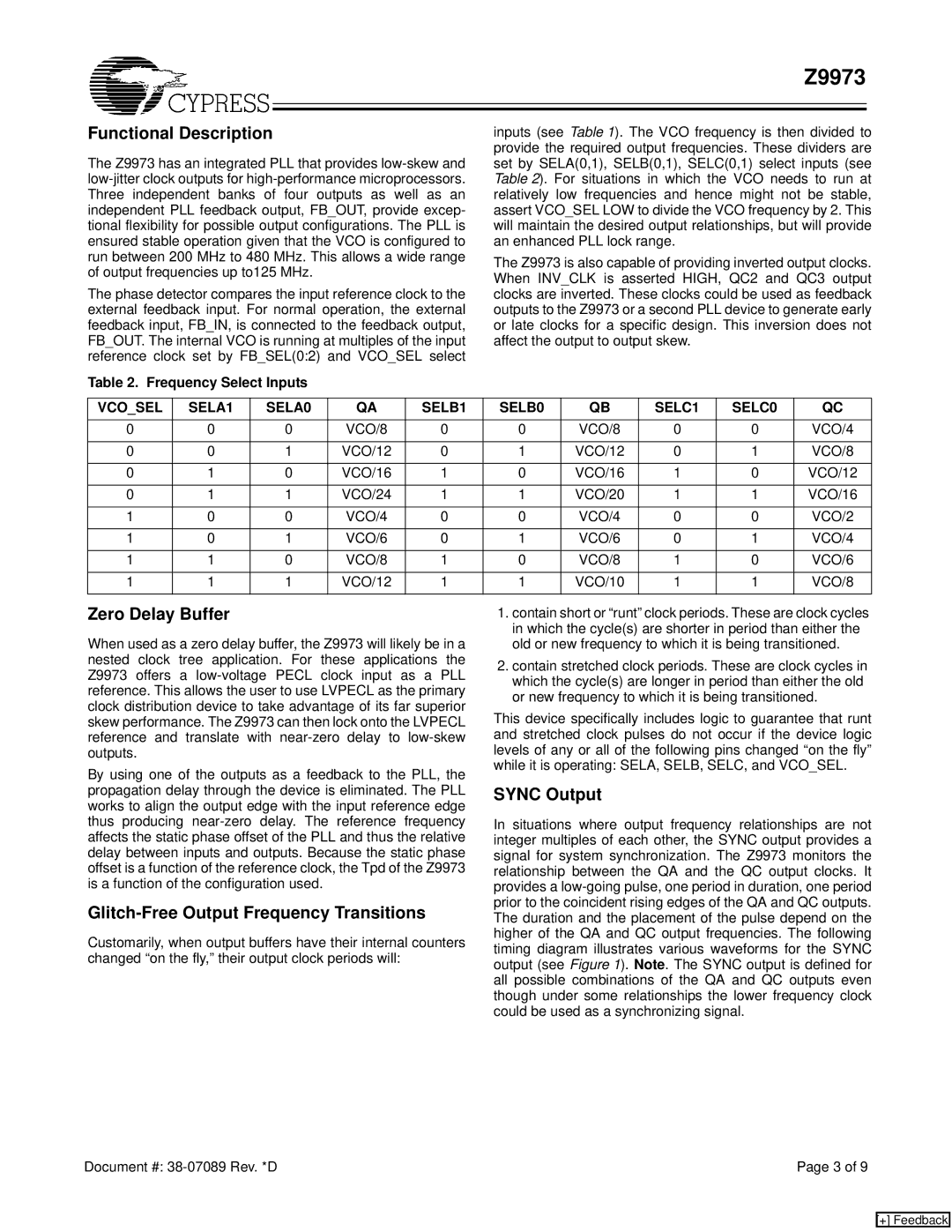
Table 2. Frequency Select Inputs
inputs (see Table 1). The VCO frequency is then divided to provide the required output frequencies. These dividers are set by SELA(0,1), SELB(0,1), SELC(0,1) select inputs (see Table 2). For situations in which the VCO needs to run at relatively low frequencies and hence might not be stable, assert VCO_SEL LOW to divide the VCO frequency by 2. This will maintain the desired output relationships, but will provide an enhanced PLL lock range.
The Z9973 is also capable of providing inverted output clocks. When INV_CLK is asserted HIGH, QC2 and QC3 output clocks are inverted. These clocks could be used as feedback outputs to the Z9973 or a second PLL device to generate early or late clocks for a specific design. This inversion does not affect the output to output skew.
VCO_SEL | SELA1 | SELA0 | QA | SELB1 | SELB0 | QB | SELC1 | SELC0 | QC |
|
|
|
|
|
|
|
|
|
|
0 | 0 | 0 | VCO/8 | 0 | 0 | VCO/8 | 0 | 0 | VCO/4 |
|
|
|
|
|
|
|
|
|
|
0 | 0 | 1 | VCO/12 | 0 | 1 | VCO/12 | 0 | 1 | VCO/8 |
|
|
|
|
|
|
|
|
|
|
0 | 1 | 0 | VCO/16 | 1 | 0 | VCO/16 | 1 | 0 | VCO/12 |
|
|
|
|
|
|
|
|
|
|
0 | 1 | 1 | VCO/24 | 1 | 1 | VCO/20 | 1 | 1 | VCO/16 |
|
|
|
|
|
|
|
|
|
|
1 | 0 | 0 | VCO/4 | 0 | 0 | VCO/4 | 0 | 0 | VCO/2 |
|
|
|
|
|
|
|
|
|
|
1 | 0 | 1 | VCO/6 | 0 | 1 | VCO/6 | 0 | 1 | VCO/4 |
|
|
|
|
|
|
|
|
|
|
1 | 1 | 0 | VCO/8 | 1 | 0 | VCO/8 | 1 | 0 | VCO/6 |
|
|
|
|
|
|
|
|
|
|
1 | 1 | 1 | VCO/12 | 1 | 1 | VCO/10 | 1 | 1 | VCO/8 |
|
|
|
|
|
|
|
|
|
|
Zero Delay Buffer
When used as a zero delay buffer, the Z9973 will likely be in a nested clock tree application. For these applications the Z9973 offers a
By using one of the outputs as a feedback to the PLL, the propagation delay through the device is eliminated. The PLL works to align the output edge with the input reference edge thus producing
Glitch-Free Output Frequency Transitions
Customarily, when output buffers have their internal counters changed “on the fly,” their output clock periods will:
1.contain short or “runt” clock periods. These are clock cycles in which the cycle(s) are shorter in period than either the old or new frequency to which it is being transitioned.
2.contain stretched clock periods. These are clock cycles in which the cycle(s) are longer in period than either the old or new frequency to which it is being transitioned.
This device specifically includes logic to guarantee that runt and stretched clock pulses do not occur if the device logic levels of any or all of the following pins changed “on the fly” while it is operating: SELA, SELB, SELC, and VCO_SEL.
SYNC Output
In situations where output frequency relationships are not integer multiples of each other, the SYNC output provides a signal for system synchronization. The Z9973 monitors the relationship between the QA and the QC output clocks. It provides a
Document #: | Page 3 of 9 |
[+] Feedback