Z9973
Power Management
The individual output enable/freeze control of the Z9973 allows the user to implement unique power management schemes into the design. The outputs are stopped in the logic “0” state when the freeze control bits are activated. The serial input register contains one programmable freeze enable bit for 12 of the 14 output clocks. The QC0 and FB_OUT outputs cannot be frozen with the serial port, which avoids any potential
serial data. An output is frozen when a logic “0” is programmed and enabled when a logic “1” is written. The enabling and freezing of individual outputs is done in such a manner as to eliminate the possibility of partial “runt” clocks.
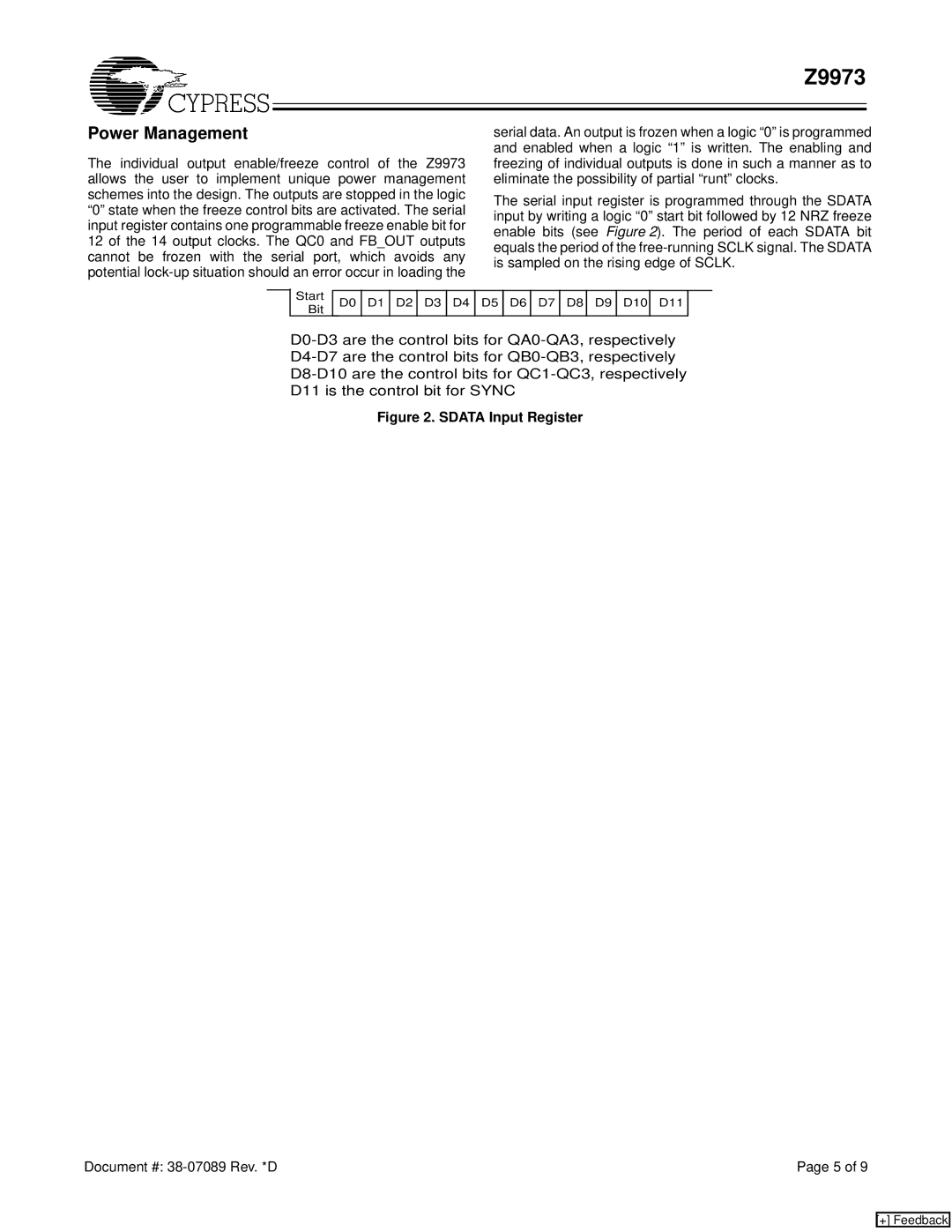
The serial input register is programmed through the SDATA input by writing a logic “0” start bit followed by 12 NRZ freeze enable bits (see Figure 2). The period of each SDATA bit equals the period of the
Start Bit
D0 D1 D2 D3 D4 D5 D6 D7 D8 D9 D10 D11
D11 is the control bit for SYNC
Figure 2. SDATA Input Register
Document #: | Page 5 of 9 |
[+] Feedback