2.8-5.5Vin, 0.75-3.3V, 10A specifications
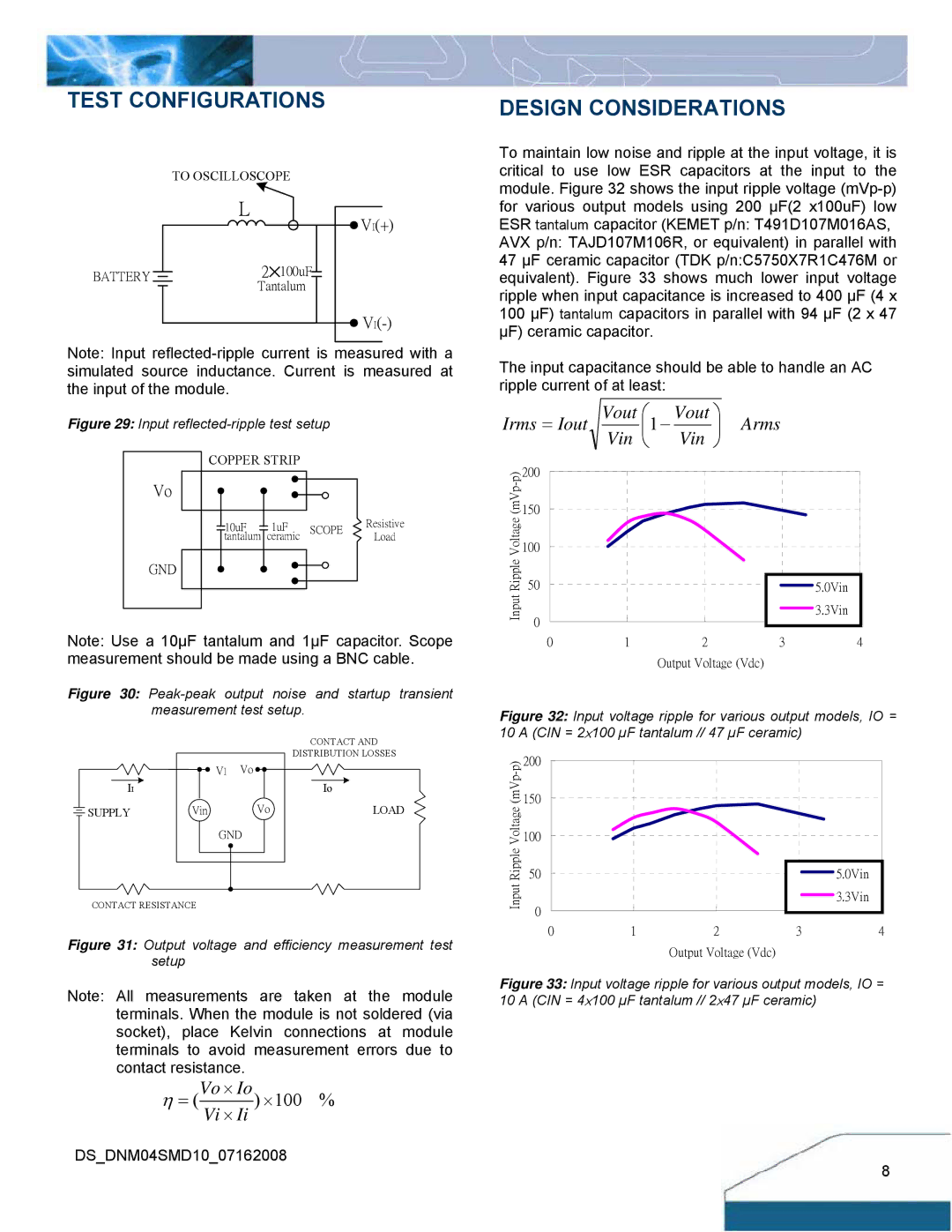
Delta Electronics has established itself as a leading provider of power supply solutions, and its latest offering, the Delta Electronics 2.8-5.5Vin, 10A, 0.75-3.3V DC-DC converter, exemplifies the company’s commitment to high efficiency and reliability in power management. This product is particularly suitable for a wide range of applications, including industrial automation, telecommunications, and consumer electronics.One of the standout features of this DC-DC converter is its wide input voltage range of 2.8 to 5.5 volts. This flexibility allows it to be used in various applications where voltage levels may vary, ensuring compatibility with different systems and reducing the need for additional voltage regulation components. The device is also capable of providing up to 10A of output current, which is ideal for powering high-demand electronic components.
The output voltage range of 0.75 to 3.3 volts makes this converter versatile for diverse operational requirements. Users can easily adjust the output voltage using external resistors, allowing for a customized power solution tailored to specific needs. This adjustability is critical in applications where components may have different voltage requirements, enhancing the overall efficiency of the power system.
Delta’s DC-DC converter employs advanced synchronous rectification technology which significantly improves efficiency by minimizing losses associated with power conversion. The converter achieves efficiencies that can exceed 90%, helping to minimize heat generation and improve the thermal performance of the entire system. This is particularly important in compact designs where space and heat dissipation are critical concerns.
Additionally, the Delta Electronics converter is designed with built-in protections, including overcurrent, overvoltage, and thermal shutdown features. These safety mechanisms ensure reliable operation even in demanding environments, safeguarding both the converter and the connected loads.
In terms of physical characteristics, the converter is packaged in a compact form factor, facilitating easy integration into various systems. Its low profile design enables it to fit into space-constrained applications without compromising on performance.
Overall, Delta Electronics’ 2.8-5.5Vin, 10A, 0.75-3.3V DC-DC converter is an excellent choice for designers seeking a dependable, efficient, and compact power solution for their diverse electronic applications. The combination of wide input voltage range, adjustable output, high efficiency, and robust protection features make it a standout product in the power management market.

