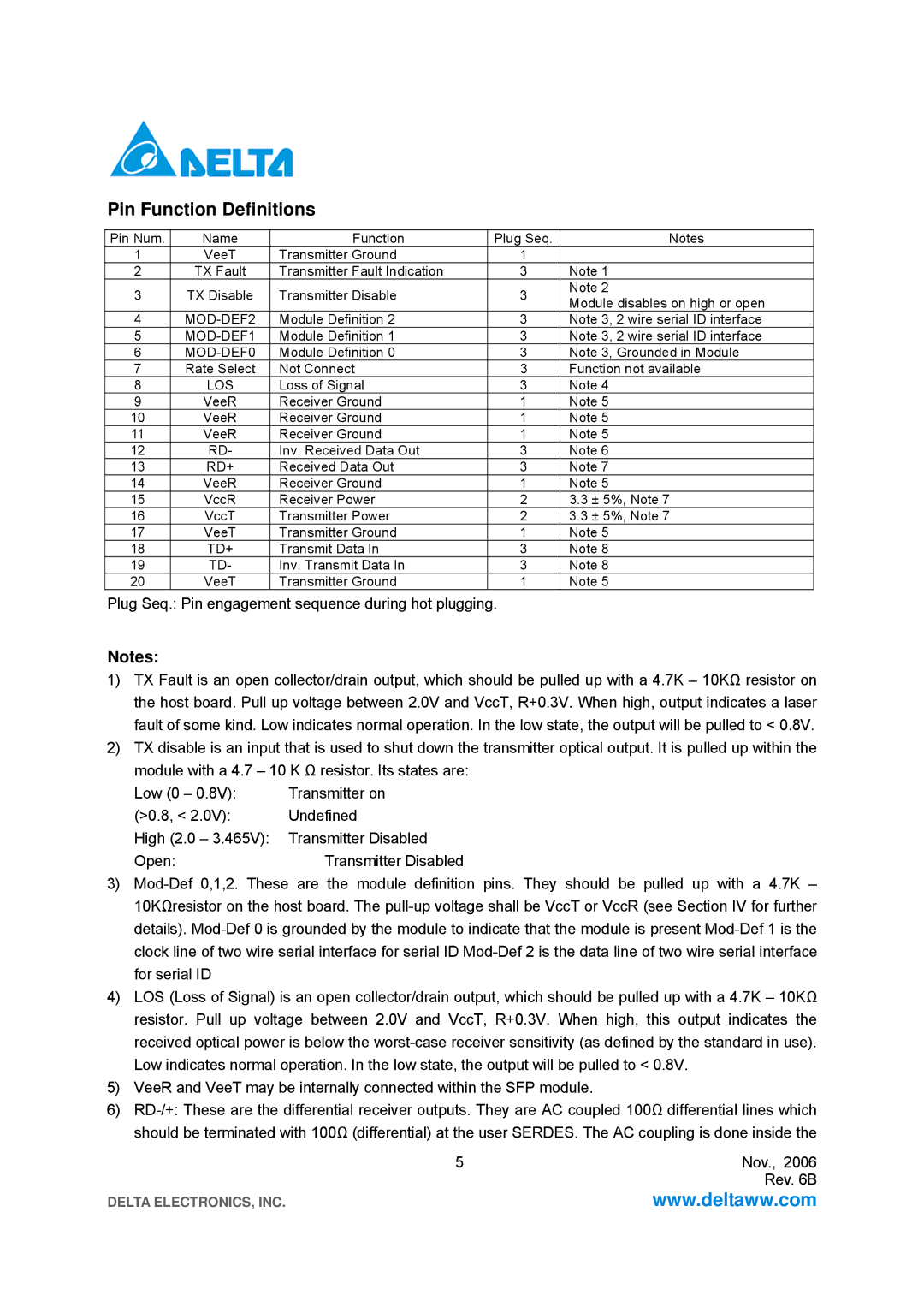
Pin Function Definitions
Pin Num. | Name | Function | Plug Seq. | Notes | |
1 | VeeT | Transmitter Ground | 1 |
| |
2 | TX Fault | Transmitter Fault Indication | 3 | Note 1 | |
3 | TX Disable | Transmitter Disable | 3 | Note 2 | |
Module disables on high or open | |||||
|
|
|
| ||
4 | Module Definition 2 | 3 | Note 3, 2 wire serial ID interface | ||
5 | Module Definition 1 | 3 | Note 3, 2 wire serial ID interface | ||
6 | Module Definition 0 | 3 | Note 3, Grounded in Module | ||
7 | Rate Select | Not Connect | 3 | Function not available | |
8 | LOS | Loss of Signal | 3 | Note 4 | |
9 | VeeR | Receiver Ground | 1 | Note 5 | |
10 | VeeR | Receiver Ground | 1 | Note 5 | |
11 | VeeR | Receiver Ground | 1 | Note 5 | |
12 | RD- | Inv. Received Data Out | 3 | Note 6 | |
13 | RD+ | Received Data Out | 3 | Note 7 | |
14 | VeeR | Receiver Ground | 1 | Note 5 | |
15 | VccR | Receiver Power | 2 | 3.3 ± 5%, Note 7 | |
16 | VccT | Transmitter Power | 2 | 3.3 ± 5%, Note 7 | |
17 | VeeT | Transmitter Ground | 1 | Note 5 | |
18 | TD+ | Transmit Data In | 3 | Note 8 | |
19 | TD- | Inv. Transmit Data In | 3 | Note 8 | |
20 | VeeT | Transmitter Ground | 1 | Note 5 |
Plug Seq.: Pin engagement sequence during hot plugging.
Notes:
1)TX Fault is an open collector/drain output, which should be pulled up with a 4.7K – 10KΩ resistor on the host board. Pull up voltage between 2.0V and VccT, R+0.3V. When high, output indicates a laser fault of some kind. Low indicates normal operation. In the low state, the output will be pulled to < 0.8V.
2)TX disable is an input that is used to shut down the transmitter optical output. It is pulled up within the module with a 4.7 – 10 K Ω resistor. Its states are:
Low (0 – 0.8V): | Transmitter on |
(>0.8, < 2.0V): | Undefined |
High (2.0 – 3.465V): | Transmitter Disabled |
Open: | Transmitter Disabled |
3)
4)LOS (Loss of Signal) is an open collector/drain output, which should be pulled up with a 4.7K – 10KΩ resistor. Pull up voltage between 2.0V and VccT, R+0.3V. When high, this output indicates the received optical power is below the
5)VeeR and VeeT may be internally connected within the SFP module.
6)
5 | Nov., 2006 |
| Rev. 6B |
DELTA ELECTRONICS, INC. | www.deltaww.com |
