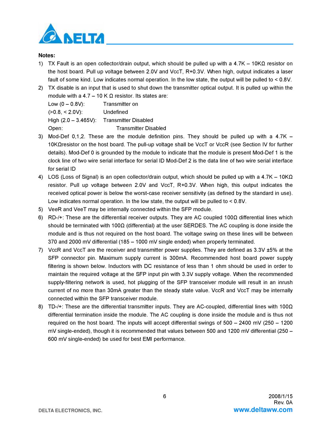
LCP-1250 CWDM specifications
Delta Electronics, a prominent leader in power and thermal management solutions, has developed the LCP-1250 CWDM (Coarse Wavelength Division Multiplexing) system, designed to enhance optical networking capabilities. This innovative solution is central to modern data centers and telecommunications, enabling efficient data transmission by using different wavelengths of light to send multiple signals over a single optical fiber.One of the main features of the LCP-1250 CWDM is its exceptional capacity to support multiple channels. By leveraging the CWDM technology, the system can transmit up to 18 channels, each operating at various wavelengths in the range of 1270nm to 1330nm. This feature allows for the simultaneous transfer of multiple data streams, significantly increasing bandwidth without the need for additional fibers. Consequently, organizations can maximize the use of their existing infrastructure, leading to reduced operational costs.
Another key characteristic of the LCP-1250 is its scalability. The modular design enables users to easily expand their networks according to growing demands. As data traffic increases, additional capacity can be integrated without requiring massive overhauls or replacements. This flexibility is essential for businesses aiming to future-proof their networking capabilities and adapt to evolving market conditions.
Moreover, Delta’s LCP-1250 utilizes advanced optical components that enhance signal quality and minimize loss. The system supports a wide variety of applications, including enterprise interconnects, metropolitan area networks, and data center interconnections. The high performance and reliability of the LCP-1250 make it an ideal solution for critical data transmission needs.
In terms of management and monitoring, the LCP-1250 comes equipped with user-friendly interfaces and software tools that facilitate real-time network performance assessment. This allows operators to monitor parameters like signal strength, channel status, and network health, leading to proactive troubleshooting and optimized performance.
The LCP-1250 CWDM also adheres to stringent environmental and regulatory standards, ensuring not only efficient operation but also sustainability. Delta Electronics focuses on energy efficiency, which helps reduce the carbon footprint of data centers while maintaining high performance levels.
In conclusion, the Delta Electronics LCP-1250 CWDM system stands out for its high capacity, scalability, advanced optical technology, and ease of management. As organizations continue to seek innovative solutions for their networking challenges, the LCP-1250 positions itself as a reliable choice for efficient optical communication.

